


FPGA Registers
EPU-4562 Programmer’s Reference Manual
21
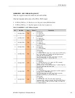
SPI
D
EBUG
C
ONTROL
R
EGISTER AND M
SATA/PCI
E
S
ELECT
C
ONTROL
R
EGISTER
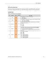
This register is only used to set an SPI loopback (debug/test only) but is also used for the
mSATA/PCIe Minicard Mux select.
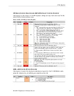
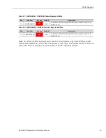
Table 15: SPI – SPI Debug Control Register
Bit
Identifier
Access
Default
Description
7
Reserved
RO
0
Reserved. Writes are ignored; reads always return 0.
6-4
MUXSEL(2:0)
R/W
000
mSATA/PCIe Mux selection for Minicard slot (and 2
nd
SATA
connector):
•
000 – Select mSATA using only pin 43 (MSATA_DETECT). This
is an Intel-mode that is reliable for PCIe Minicards but not for
mSATA modules that inadvertently ground this signal.
•
001 – Use only Pin 51 (PRES_DISABLE2#). This is the default
method and is defined in the Draft mSATA spec but some
Minicards use it as a second wireless disable.
•
010 – Use either Pin 43 or Pin 51. This will work just like 001
because Pin 43 is disabled by an FPGA pull-down.
•
011 – Force PCIe mode on the Minicard
•
100 – Force mSATA mode on the Minicard.
•
101 – Undefined (same as 000)
•
110 – Undefined (same as 000)
•
111 – Undefined (same as 000)
Note:
When the Minicard uses PCIe, the SATA channel automatically
switches to the SATA connector.
3
Reserved
RO
0
Reserved. Writes are ignored; reads always return 0.
2
SERIRQEN
R/W
0
When an IRQ is assigned a slot in the SERIRQ, it will drive the slot
with the interrupt state, but this bit must be set to a ‘1’ to do that.
0 – Slots assigned to SERIRQ are not driven (available for other
devices).
1 – Slots assigned to SERIRQ are driven with their current interrupt
state (which is low since interrupts are high-true).
This is because the default interrupt settings in this FPGA can conflict
with other interrupts if the VersaAPI is not being used (for example,
console redirect using IRQ3).
1
SPILB
R/W
0
Debug/Test Only: Used to loop SPI output data back to the input
(debug/test mode).
0 – Normal operation
1 – Loop SPI output data back to the SPI input data (data output still
active)
0
Reserved
RO
0
Reserved. Writes are ignored; reads always return 0.
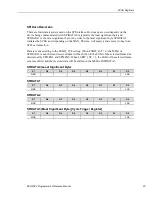
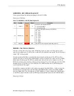
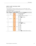
ADM
–
ADC
C
ONTROL
/S
TATUS
R
EGISTER
This register is used as the interrupt control/status register for the TI ADS8668A and is
primarily related to the ALARM signal output from the A/
D
.
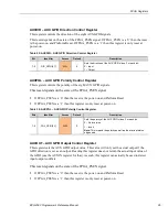
Bit
Identifier
Access
Default
Description
7
IRQEN
R/W
0
ADC ALARM Interrupt Enable/Disable.
0 – Interrupts disabled
1 – Interrupts enabled.
Note: This is essentially the interrupt mask.