TE0600 TRM
Revision: V3.02
Copyright © 2017 Trenz Electronic GmbH
Page of
8
33
http://www.trenz-electronic.de
We recommend to supply the module with all these 14 pins. When one or more of these pins are not power
supplied, it or they can be used as power source for user applications.
Please make sure that your logic design does not draw more RMS current per pin than specified in section
.
Board-to-board Connectors
FPGA banks VCCIO power supply
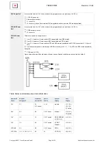
FPGA VCCIO power options are shown below. Default values for configurable voltages are shown in
braces.
Bank
Supply voltage
B0
VCCIO 0 (3.3 V)
B1
VCCIO 1 (1.5 V)
B2
3.3 V
B3
1.5 V
Bank 0 power supply VCCIO 0 can be configured by user to 3.3 V, 2.5 V or 1.5 V, see Chapter
VCCIO0
. Bank 1 VCCIO supply voltage is configured to 1.5 V to communicate with DDR3 SDRAM
Power Rail
memory chip.
By special request, modules can be supplied without DDR3 SDRAM chips. Contact Trenz Electronic
support for details.
On-board Power Rails
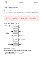
GigaBee XC6SLX has the following power rails on-board.
3.3V Power Rail
It is the main internal power rail and must be supplied from an external power source.
It supplies the other following power rails:
1.2V / 4 A on-board high-efficiency switching voltage regulator;
1.5V / 1.5 A on-board high-efficiency switching voltage regulator;
2.5V 0.8 A linear voltage regulator;
VCCIO0 power rail (option) (if zero-resistor R80 is
populated and zero-resistor R79 populated).
not
is
1.2V Power Rail
It is converted from the 3.3V rail by a switching voltage regulator and can provide up to 4.0 A to:
FPGA VCCINT power supply pins;
Ethernet PHY;
J1 connector.
1.5V Power Rail
It is converted from the 3.3V rail by a switching voltage regulator and can provide up to 1.5 A to:
DDR3 SDRAM;
Vref1 / Vref2 DDR3 SDRAM reference voltages;
FPGA bank 3 VCCO;
J1 connector.


