TE0600 TRM
Revision: V3.02
Copyright © 2017 Trenz Electronic GmbH
Page
of
24
33
http://www.trenz-electronic.de
81
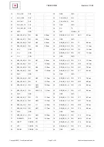
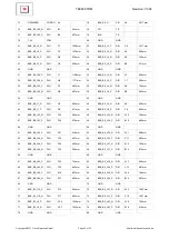
B2B_B1_L21_N
DIO
J16
13.22mm
82
B2B_B0_L64_N
DIO
A17
9.55mm
83
B2B_B1_L21_P
DIO
K16
14.41mm
84
B2B_B0_L64_P
DIO
C17
10.25mm
85
B2B_B1_L61_P
DIO
L17
14.89mm
86
B2B_B0_L65_N
DIO
A18
8.51mm
87
B2B_B1_L61_N
DIO
K18
13.59mm
88
B2B_B0_L65_P
DIO
B18
9.29mm
89
GND
GND
-
-
90
GND
GND
-
-
91
VCCAUX
POW
-
-
92
B2B_B1_L20_P
DIO
A20
8.02mm
93
TMS
JTAG
C18
-
94
B2B_B1_L20_N
DIO
A21
7.82mm
95
TDI
JTAG
E18
-
96
B2B_B1_L19_P
DIO
B21
9.63mm
97
TDO
JTAG
A19
-
98
B2B_B1_L19_N
DIO
B22
9.06mm
99
TCK
JTAG
G15
-
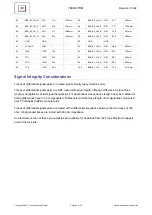
100
B2B_B1_L59
SIO
P19
27.19mm
Signal Integrity Considerations
Traces of differential signals pairs are routed symmetrically (as symmetric pairs).
Traces of differential signals pairs are NOT routed with equal length, although difference in signal lines
length is negligible for actual signal frequencies. For applications where traces length has to be matched or
timing differences have to be compensated, Tables below list the trace length of I/O signal lines measured
from FPGA balls to B2B connector pins.
Traces of differential signals pairs are routed with a differential impedance between the two traces of 100
ohm. Single ended traces are routed with 60 ohm impedance.
An electronic version of these pin-out tables are available for download from the Trenz Electronic support
area of the web site.

