1-11-5
E9TK3TR
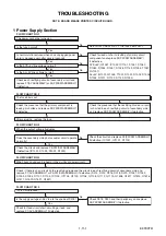
Yes
Yes
Yes
Yes
No
No
No
No
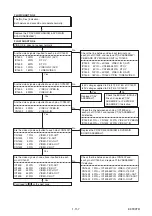
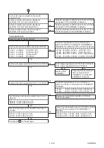
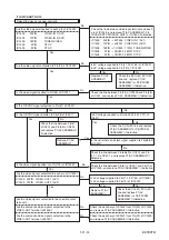
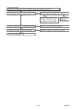
The fluorescent display tube does not light up.
Is 5V voltage supplied to Pin(13,43) of IC612?
Is approximately -24V to -28V voltage supplied to
Pin(30) of IC612?
Is there approximately 500kHz oscillation to
Pin(5) of IC612?
Are the filament voltage applied between Pin(1)
and Pin(24) of the fluorescent display tube?
Also negative voltage applied between these pins
and GND?
Replace P1(AV ASSEMBLY).
Check the ECO+5V line and replace
P1(AV ASSEMBLY) if defective.
Check the -FL line and replace P1(AV ASSEMBLY)
or P4(PW/SW ASSEMBLY) if defective.
Check R618, IC612 and their periphery, and replace
P1(AV ASSEMBLY) if defective.
Check the power circuit, D1103, D1108, R1106, R1192,
C1110 and their periphery, and replace
P4(PW/SW ASSEMBLY) if defective.
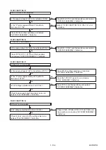
FLOW CHART NO.21
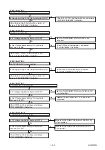
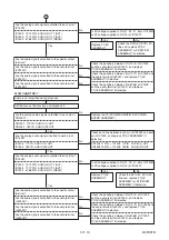
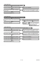
Check IC1103 and their periohery, and replace
P1(AV ASSEMBLY) if defective.
FLOW CHART NO.19
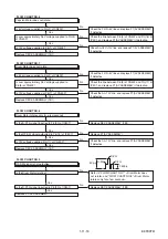
P-ON+1.8V is not outputted.
Is 2.5V voltage supplied to pin(1) of IC1103?
No
Yes
Yes
Check D1033 and their periohery, and replace
P4(PW/SW ASSEMBLY) if defective.
No
Check IC3607(IC3608) and their periphery, and
replace P4(PW/SW ASSEMBLY) if defective.
No
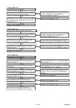
Is 5V voltage supplied to Pin(4) of CN6001?
When IC3607 is used:
Is 5V voltage outputted to Pin(8) of IC3607?
When IC3608 is used:
Is 5V voltage outputted to Pin(5) of IC3608?
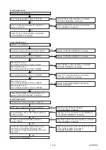
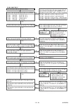
FLOW CHART NO.20
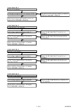
USB+5V is not outputted.
Is resistance value of both end to F6001 infinity?
Replace P4(PW/SW ASSEMBLY) if defective.
Yes
No
Replace P4(PW/SW ASSEMBLY) if defective.
Yes
Check CN3604 and their periphery, and replace
P4(PW/SW ASSEMBLY) if defective.
Yes
Check Q1119 and their periphery, and replace
P4(PW/SW ASSEMBLY) if defective.
Is 0V voltage outputted to Pin(1) of CN3605?
No
Yes
No
When IC3607 is used:
Is 3.3V voltage supplied to Pin(4) of IC3607?
When IC3608 is used:
Is 3.3V voltage supplied to Pin(3) of IC3608?
Yes
Replace P2(DVD MECHANISM & DVD MAIN
BOARD ASSEMBLY).
Is the "H" pulse (approximately 5V) inputted to
the base of Q1109?
Check the REG-CONT signal line, and replace
P1(AV ASSEMBLY) if defective.
No
Summary of Contents for DVR19DTKB2
Page 4: ...1 1 1 E9TK3SP SPECIFICATIONS ...
Page 58: ...1 14 3 NOTE BOARD MEANS PRINTED CIRCUIT BOARD E9TK3SCAV1 AV 1 9 Schematic Diagram VCR Section ...
Page 60: ...1 14 5 NOTE BOARD MEANS PRINTED CIRCUIT BOARD E9TK3SCAV3 AV 3 9 Schematic Diagram VCR Section ...
Page 61: ...1 14 6 NOTE BOARD MEANS PRINTED CIRCUIT BOARD E9TK3SCAV4 AV 4 9 Schematic Diagram VCR Section ...
Page 62: ...1 14 7 NOTE BOARD MEANS PRINTED CIRCUIT BOARD E9TK3SCAV5 AV 5 9 Schematic Diagram VCR Section ...
Page 63: ...1 14 8 NOTE BOARD MEANS PRINTED CIRCUIT BOARD E9TK3SCAV6 AV 6 9 Schematic Diagram VCR Section ...
Page 64: ...1 14 9 NOTE BOARD MEANS PRINTED CIRCUIT BOARD E9TK3SCAV7 AV 7 9 Schematic Diagram VCR Section ...
Page 89: ...1 17 3 DVDP_TI Push close 0 08 V 0 02 s Push Close detection Threshold level ...
Page 97: ...1 20 4 E9TK3PEX Packing X 2 X 3 X 6 X1 Upper Side Lower Side FRONT ...
Page 123: ......

