


SM320F2812-HT
SGUS062B
–
JUNE 2009
–
REVISED JUNE 2011
www.ti.com
6
Electrical Specifications
This section provides the absolute maximum ratings and the recommended operating conditions for the
SM/SMJ320F2812 DSP.
6.1
Absolute Maximum Ratings
Unless otherwise noted, the list of absolute maximum ratings are specified over operating temperature
ranges. Stresses beyond those listed under Absolute Maximum Ratings may cause permanent damage to
the device. These are stress ratings only, and functional operation of the device at these or any other
conditions beyond those indicated under
Section 6.2
is not implied. Exposure to absolute-maximum-rated
conditions for extended periods may affect device reliability. All voltage values are with respect to V
SS
.
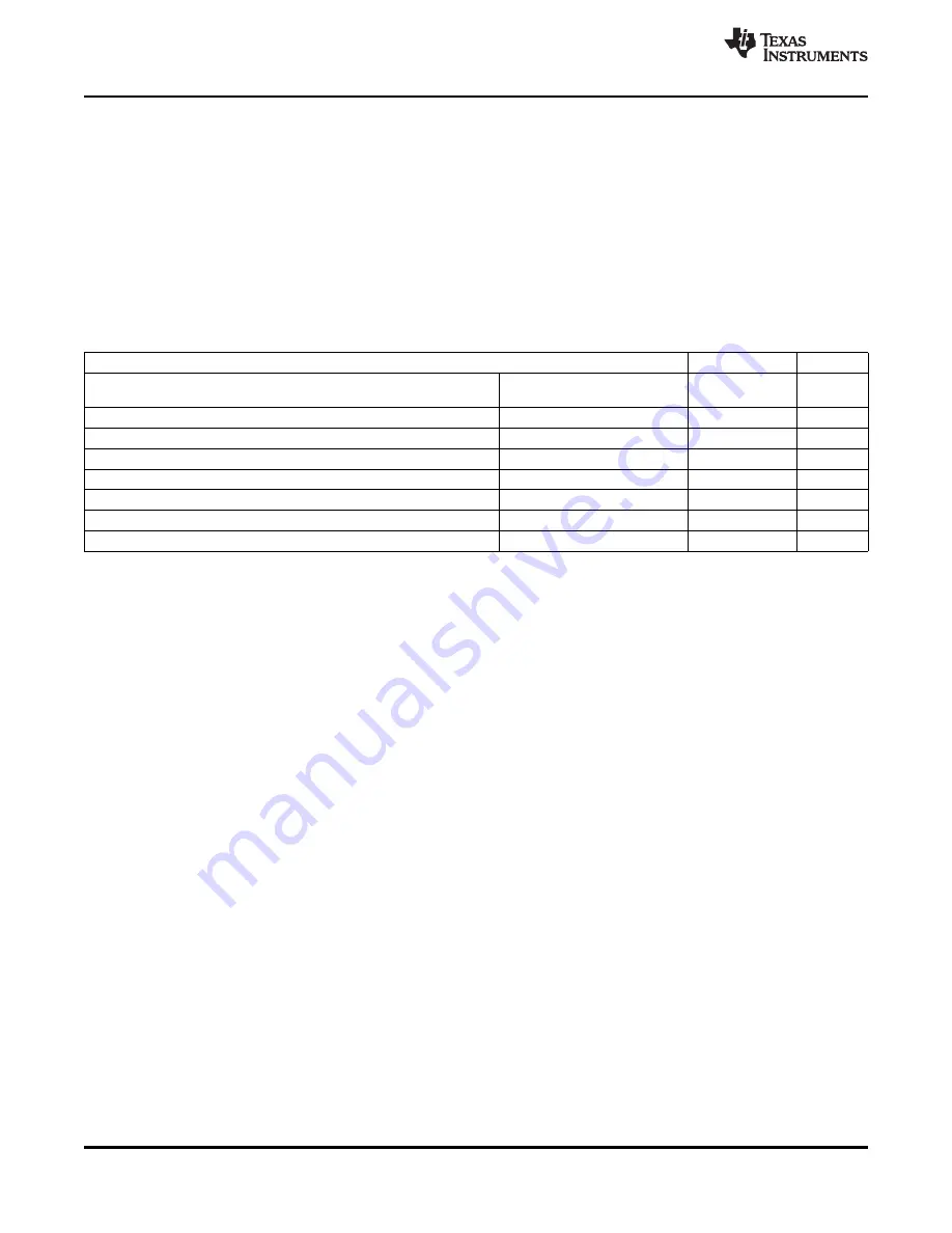
xxx
VALUE
UNIT
Supply voltage range, V
DDIO
, V
DDA1
, V
DDA2
, V
DDAIO
, and
–
0.3 to 4.6
V
AV
DDREFBG
Supply voltage range, V
DD
, V
DD1
–
0.5 to 2.5
V
V
DD3VFL
range
–
0.3 to 4.6
V
Input voltage range, V
IN
–
0.3 to 4.6
V
Output voltage range, V
O
–
0.3 to 4.6
V
Input clamp current, I
IK
(V
IN
<
0 or V
IN
>
V
DDIO
)
(1)
±
20
mA
Output clamp current, I
OK
(V
O
<
0 or V
O
>
V
DDIO
)
±
20
mA
Operating ambient temperature range, T
A
(2)
S Temp
–
55 to 220
°
C
(1)
Continuous clamp current per pin is
±
2 mA
(2)
Long-term high-temperature storage and/or extended use at maximum temperature conditions may result in a reduction of overall device
life.
84
Electrical Specifications
Copyright
©
2009
–
2011, Texas Instruments Incorporated
Submit Documentation Feedback
Product Folder Link(s):
SM320F2812-HT
Summary of Contents for SM320F2812-HT Data
Page 152: ......


