Texas Instruments DRV2700EVM-HV500 User Manual Download Page 13

=

FB1

FB2

FB2

FB1

R

C

R

C

=

æ

ö

æ

ö

+

-

ç

÷

ç

÷

è

ø

è

ø

FB1

FB1

HV

FB

OP

FB2

FB2

V

V

V

R

R

1

R

R

C

(FB1)

C

(FB2)

R

(FB2A)

R

(FB2B)

V

HV

Pull down 

Reference

Filte r O utp ut

V

FB

www.ti.com

Flyback Converter

4.1

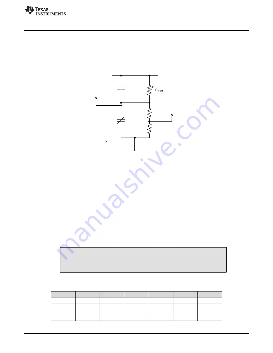
Programming the HV Maximum Output Voltage

The high voltage output (HV) is set through an external network. For ease-of-use of this EVM, two
switches (SW3 and SW4) are installed to change R

FB1

and C

FB2

with ease. For a normal application,

switches should not be needed and those values can be set by passives.

Additionally, R

FB2

is split into two resistors to provide a reference voltage for the pull-down operational

amplifier (opamp) that is discussed in

Pulldown Network

.

Figure 9. V

HV

Feedback Network

The HV output voltage is given by:

Equation 2

(1)

where V

FB

= 1.30 V and V

OP

is the V

OL

of the opamp since it cannot go all the way to ground. TI

recommends the sum of the resistance of R

FB1

and R

FB2

be between 500 k

Ω

and 1 M

Ω

.

The capacitors are needed in the feedback network to increase the performance at low and high
frequencies. Because the charge storage is inversely proportional to the capacitance, use

Equation 2

to

calculate the values of the capacitors. In general, select a value around 22 pF for C

FB1

and size C

FB2

accordingly.

(2)

Refer to

Table 3

for the switch setting to change the maximum output voltage.

CAUTION

Be sure not to hot switch the SW3 and SW4 connection. This should only be
switched while the output is disabled or the board is unpowered.

Table 3. V

HV

Setting Based on the Jumper Configuration

SW3

SW4

R

FB2

C

FB2

R

FB1

C

FB1

V

MAX

Down

Down

5.49 k

Ω

8200 pF

2.05 M

Ω

22 pF

500 V

Down

Up

5.49 k

Ω

4505 pF

1.122 M

Ω

22 pF

275 V

Up

Down

5.49 k

Ω

3717 pF

0.866 M

Ω

22 pF

212 V

Up

Down

5.49 k

Ω

2710 pF

0.642 M

Ω

22 pF

158 V

13

SLOU407A – April 2015 – Revised May 2015

DRV2700EVM-HV500 High Voltage Piezo Driver Evaluation Kit

Submit Documentation Feedback

Copyright © 2015, Texas Instruments Incorporated

Summary of Contents for DRV2700EVM-HV500

Page 1: ...all around use and can be used not only for evaluation but can also be used for prototyping into systems for driving piezo actuators polymers valves and many other applications The EVM also contains a...

Page 2: ...2 Pulldown Network 17 7 Input Filter 19 7 1 First Order Filter 19 7 2 Integrator 19 8 Reference 20 8 1 Schematic 20 8 2 PCB Layout 21 8 3 Bill of Materials 22 List of Figures 1 Board Diagram 6 2 Powe...

Page 3: ...rization from U S Department of Commerce and other competent Government authorities to the extent required by those laws This provision shall survive termination or expiration of this Agreement Accord...

Page 4: ...OLTAGE Danger High Voltage Electric shock possible when connecting board to live wire Board should be handled with care by a professional For safety use of isolated test equipment with overvoltage ove...

Page 5: ...ccess d All interface circuits power supplies evaluation modules instruments meters scopes and other related apparatus used in a development environment exceeding 50Vrms 75VDC must be electrically loc...

Page 6: ...er up The MSP430 has each of these control settings low which disables the DRV2700 by default Figure 1 shows the basic board diagram of the DRV2700EVM HV500 Table 2 shows the original configuration of...

Page 7: ...cted to either power supply JP4 DRV VIN 1 DRV2700 connected to VIN power supply USB 1 X DRV2700 connected to USB power supply Open EN pulled internally to GND through DRV2700 internal resistance JP3 E...

Page 8: ...from a standard USB port on a computer USB charger or USB battery pack This input is intended for ease of use and can be routed to power all circuitry on the EVM Additionally this input has a 5 V LED...

Page 9: ...level high 2 5 Inputs The analog input TP1 is used for PWM and analog inputs See PWM and Analog Inputs for more information 2 6 Outputs The DRV2700EVM HV500 has a high voltage output ranging from 0 5...

Page 10: ...ontrol Software GUI By default the DRV2700EVM HV500 can be controlled programmatically through the GUI Interface Figure 4 is a screenshot of the GUI Run the GUI by downloading it from the DRV2700EVM H...

Page 11: ...his will cause the output to try and reflect the PWM signal coming from the microcontroller and the output will try to be a square wave The AC Mode Quick Launch frequency button will set the frequency...

Page 12: ...ize switching losses and therefore increase efficiency A hysteretic controller is a self oscillation circuit that regulates the output voltage by keeping the output voltage within a hysteresis window...

Page 13: ...e resistance of RFB1 and RFB2 be between 500 k and 1 M The capacitors are needed in the feedback network to increase the performance at low and high frequencies Because the charge storage is inversely...

Page 14: ...ill increase the parasitic inductor losses Another factor to consider for transformers is the winding ratio In general if a 200 V output is desired then because the SW node can boost up to 100 V a tra...

Page 15: ...ge the PWM signal will be attenuated but it will still somewhat reflect a PWM signal This mode can be used for audio tones however the output may not be able to drive to full scale depending on the lo...

Page 16: ...the middle header of JP3 3 Connect the analog input signal to TP1 INPUT Note the default input range is from 0 3 3 V same as PWM signal Therefore if a voltage divider is needed R21 and R2 can be chan...

Page 17: ...Additionally placing a resistor in series with this FET on the source side to limit the current going through the FET is recommended This resistor can be sized according to the maximum current allowed...

Page 18: ...feedback network will be changed so this reference will become higher than VREXT and therefore turn on the output FET Figure 14 Pulldown Network Figure 15 and Figure 16 show the different discharge ti...

Page 19: ...ions The filter can be modified by the user however be sure that the 3 dB point is no higher than 5 kHz See scopeshots in Section 3 for example waveforms 7 1 First Order Filter In order to attenuate t...

Page 20: ...6 SW 7 SW 8 NC 9 VBST 10 VBST 11 PVDD 12 OUT 13 OUT 14 REXT 15 IN 16 IN 17 GAIN0 18 GAIN1 19 EN 20 PAD 21 U2 DRV2700RGP GND 0 1 F C3 GND 0 1uF C9 GND GND Green D3 511 R13 EN 3 3k R7 GND 1 2 3 JP3 VRES...

Page 21: ...shows the DRV2700EVM HV500 PCB layout Figure 19 Top and Bottom Layers 21 SLOU407A April 2015 Revised May 2015 DRV2700EVM HV500 High Voltage Piezo Driver Evaluation Kit Submit Documentation Feedback C...

Page 22: ...rata 0402 C19 1 6800pF CAP CERM 6800 pF 25 V 10 X7R 0402 GRM155R71E682KA01D Murata 0402 C20 C24 C26 3 0 1uF CAP CERM 0 1uF 6 3V 10 X5R 0402 0402 C1005X5R0J104K TDK C21 1 8200pF CAP CERM 8200 pF 16 V 1...

Page 23: ...210K0JNED Vishay Dale R16 R17 2 33 RES 33 ohm 5 0 063W 0402 0402 CRCW040233R0JNED Vishay Dale R18 1 392 RES 392 1 0 063 W 0402 0402 CRCW0402392RFKED Vishay Dale R19 1 9 76k RES 9 76k ohm 1 0 063W 0402...

Page 24: ...alent None Output 2 to 5 5 V Input with Low IQ 5 pin SC70 DCK 40 to 125 degC Green RoHS no Sb Br U5 1 Mixed Signal MicroController RGZ0048A RGZ0048A MSP430F5510IRGZ Texas Instruments None Y1 1 CRYSTAL...

Page 25: ...to A Revision Page Changed GUI Interface image 10 NOTE Page numbers for previous revisions may differ from page numbers in the current version 25 SLOU407A April 2015 Revised May 2015 Revision History...

Page 26: ...ing the warranty period to the address designated by TI and that are determined by TI not to conform to such warranty If TI elects to repair or replace such EVM TI shall have a reasonable time to repa...

Page 27: ...transmitter has been approved by Industry Canada to operate with the antenna types listed in the user guide with the maximum permissible gain and required antenna impedance for each antenna type indic...

Page 28: ...ified allowable ranges some circuit components may have elevated case temperatures These components include but are not limited to linear regulators switching transistors pass transistors current sens...

Page 29: ...REMOVAL OR REINSTALLATION ANCILLARY COSTS TO THE PROCUREMENT OF SUBSTITUTE GOODS OR SERVICES RETESTING OUTSIDE COMPUTER TIME LABOR COSTS LOSS OF GOODWILL LOSS OF PROFITS LOSS OF SAVINGS LOSS OF USE L...

Page 30: ...sponsible for compliance with all legal regulatory and safety related requirements concerning its products and any use of TI components in its applications notwithstanding any applications related inf...

Reviews: