background image

CC2500

SWRS040C

Page 1 of 89

CC2500

Low-Cost Low-Power 2.4 GHz RF Transceiver

Applications

2400-2483.5 MHz ISM/SRD band systems

Consumer electronics

Wireless game controllers

Wireless audio

Wireless keyboard and mouse

RF enabled remote controls

Product Description

The

CC2500

is a low-cost 2.4 GHz transceiver

designed for very low-power wireless appli-
cations. The circuit is intended for the 2400-
2483.5 MHz ISM (Industrial, Scientific and
Medical) and SRD (Short Range Device)
frequency band.

The RF transceiver is integrated with a highly
configurable baseband modem. The modem
supports various modulation formats and has
a configurable data rate up to 500 kBaud.

CC2500

provides extensive hardware support

for packet handling, data buffering, burst
transmissions, clear channel assessment, link
quality indication, and wake-on-radio.

The main operating parameters and the 64-
byte transmit/receive FIFOs of

CC2500

can be

controlled via an SPI interface. In a typical
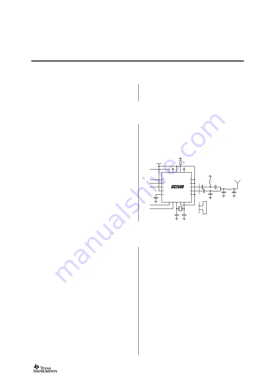
system, the

CC2500

will be used together with

a microcontroller and a few additional passive
components.

6

7

8

9

1

0

2

0

1

9

1

8

1

7

1

6

Key Features

RF Performance

High sensitivity (–104 dBm at 2.4 kBaud,
1% packet error rate)

Low current consumption (13.3 mA in RX,
250 kBaud, input well above sensitivity
limit)

Programmable output power up to +1 dBm

Excellent receiver selectivity and blocking
performance

Programmable data rate from 1.2 to 500
kBaud

Frequency range: 2400 – 2483.5 MHz

Analog Features

OOK, 2-FSK, GFSK, and MSK supported

Suitable for frequency hopping and multi-
channel systems due to a fast settling

frequency synthesizer with 90 us settling
time

Automatic

Frequency

Compensation

(AFC) can be used to align the frequency
synthesizer

to

the

received

centre

frequency

Integrated analog temperature sensor

Digital Features

Flexible

support

for

packet

oriented

systems: On-chip support for sync word
detection, address check, flexible packet
length, and automatic CRC handling

Efficient SPI interface: All registers can be
programmed with one “burst” transfer

Digital RSSI output

Programmable channel filter bandwidth

Programmable

Carrier

Sense

(CS)

indicator

Summary of Contents for CC2500

Page 1: ...ypical system the CC2500 will be used together with a microcontroller and a few additional passive components 6 7 8 9 10 20 19 18 17 16 Key Features RF Performance High sensitivity 104 dBm at 2 4 kBaud 1 packet error rate Low current consumption 13 3 mA in RX 250 kBaud input well above sensitivity limit Programmable output power up to 1 dBm Excellent receiver selectivity and blocking performance P...

Page 2: ...EEP to RX or TX mode measured on EM design Wake on radio functionality for automatic low power RX polling Separate 64 byte RX and TX data FIFOs enables burst mode data transmission General Few external components Complete on chip frequency synthesizer no external filters or RF switch needed Green package RoHS compliant and no antimony or bromine Small size QLP 4x4 mm package 20 pins Suited for sys...

Page 3: ...rent RCOSC RC Oscillator DVGA Digital Variable Gain Amplifier QPSK Quadrature Phase Shift Keying ESR Equivalent Series Resistance QLP Quad Leadless Package FCC Federal Communications Commission RC Resistor Capacitor FEC Forward Error Correction RF Radio Frequency FIFO First In First Out RSSI Received Signal Strength Indicator FHSS Frequency Hopping Spread Spectrum RX Receive Receive Mode 2 FSK Fre...

Page 4: ...E 20 10 4 WIRE SERIAL CONFIGURATION AND DATA INTERFACE 21 10 1 CHIP STATUS BYTE 22 10 2 REGISTER ACCESS 23 10 3 SPI READ 23 10 4 COMMAND STROBES 24 10 5 FIFO ACCESS 24 10 6 PATABLE ACCESS 24 11 MICROCONTROLLER INTERFACE AND PIN CONFIGURATION 25 11 1 CONFIGURATION INTERFACE 25 11 2 GENERAL CONTROL AND STATUS PINS 25 11 3 OPTIONAL RADIO CONTROL FEATURE 26 12 DATA RATE PROGRAMMING 26 13 RECEIVER CHAN...

Page 5: ...0 28 PCB LAYOUT RECOMMENDATIONS 51 29 GENERAL PURPOSE TEST OUTPUT CONTROL PINS 52 30 ASYNCHRONOUS AND SYNCHRONOUS SERIAL OPERATION 54 30 1 ASYNCHRONOUS OPERATION 54 30 2 SYNCHRONOUS SERIAL OPERATION 54 31 SYSTEM CONSIDERATIONS AND GUIDELINES 54 31 1 SRD REGULATIONS 54 31 2 FREQUENCY HOPPING AND MULTI CHANNEL SYSTEMS 55 31 3 WIDEBAND MODULATION NOT USING SPREAD SPECTRUM 55 31 4 DATA BURST TRANSMISS...

Page 6: ...V According to JEDEC STD 22 method A114 Human Body Model Table 1 Absolute Maximum Ratings 2 Operating Conditions The CC2500 operating conditions are listed in Table 2 below Parameter Min Max Unit Condition Note Operating temperature 40 85 C Operating supply voltage 1 8 3 6 V All supply pins must have the same voltage Table 2 Operating Conditions 3 General Characteristics Parameter Min Typ Max Unit...

Page 7: ...keup Average current with signal in channel below carrier sense level MCSM2 RX_TIME_RSSI 1 34 A Same as above but with signal in channel above carrier sense level 29 3 ms RX timeout and no preamble sync word found 1 5 mA Only voltage regulator to digital part and crystal oscillator running IDLE state Current consumption 7 4 mA Only the frequency synthesizer is running FSTXON state This current con...

Page 8: ... 89 11 1 mA Transmit mode 12 dBm output power 15 0 mA Transmit mode 6 dBm output power 21 2 mA Transmit mode 0 dBm output power Current consumption TX states 21 5 mA Transmit mode 1 dBm output power Table 4 Current Consumption ...

Page 9: ... Desired channel 3 dB above the sensitivity limit 250 kHz channel spacing See Figure 22 for plot of selectivity versus frequency offset Blocking 10 MHz offset 20 MHz offset 50 MHz offset 64 70 71 dBm dBm dBm Wanted signal 3 dB above sensitivity level Compliant with ETSI EN 300 440 class 2 receiver requirements 10 kBaud data rate sensitivity optimized MDMCFG2 DEM_DCFILT_OFF 0 2 FSK 1 packet error r...

Page 10: ... rejection 30 dB Desired channel 3 dB above the sensitivity limit 750 kHz channel spacing See Figure 25 for plot of selectivity versus frequency offset Blocking 10 MHz offset 20 MHz offset 50 MHz offset 46 52 55 dB dB dB Wanted signal 3 dB above sensitivity level Compliant with ETSI EN 300 440 class 2 receiver requirements 500 kBaud data rate MDMCFG2 DEM_DCFILT_OFF 0 MDMCFG2 DEM_DCFILT_OFF 1 canno...

Page 11: ...nce design 4 RF matching network It is possible to program less than 30 dBm output power but this is not recommended due to large variation in output power across operating conditions and processing corners for these settings Occupied bandwidth 99 91 117 296 489 kHz kHz kHz kHz 2 4 kBaud 38 2 kHz deviation 2 FSK 10 kBaud 38 2 kHz deviation 2 FSK 250 kBaud MSK 500 kBaud MSK Adjacent channel power A...

Page 12: ...ment results obtained using the CC2500EM reference design 4 Parameter Min Typ Max Unit Condition Note Calibrated frequency 34 7 34 7 36 kHz Calibrated RC oscillator frequency is XTAL frequency divided by 750 Frequency accuracy after calibration 1 10 The RC oscillator contains an error in the calibration routine that statistically occurs in 17 3 of all calibrations performed The given maximum accur...

Page 13: ...100 kHz offset from carrier 81 dBc Hz 200 kHz offset from carrier 90 dBc Hz 500 kHz offset from carrier 100 dBc Hz 1 MHz offset from carrier 108 dBc Hz 2 MHz offset from carrier 114 dBc Hz 5 MHz offset from carrier RF carrier phase noise 118 dBc Hz 10 MHz offset from carrier PLL turn on hop time 85 1 88 4 88 4 s Time from leaving the IDLE state until arriving in the RX FSTXON or TX state when not ...

Page 14: ...se when enabled 0 3 mA Table 10 Analog Temperature Sensor Parameters 4 8 DC Characteristics Tc 25 C if nothing else stated Digital Inputs Outputs Min Max Unit Condition Note Logic 0 input voltage 0 0 7 V Logic 1 input voltage VDD 0 7 VDD V Logic 0 output voltage 0 0 5 V For up to 4 mA output current Logic 1 output voltage VDD 0 3 VDD V For up to 4 mA output current Logic 0 input current N A 50 nA ...

Page 15: ...4 3 2 GND Exposed die attach pad SCLK SO GDO1 GDO2 DVDD DCOUPL GDO0 ATEST XOSC_Q1 AVDD XOSC_Q2 AVDD RF_P RF_N GND AVDD RBIAS DGUARD GND SI CSn AVDD Figure 1 Pinout Top View Note The exposed die attach pad must be connected to a solid ground plane as this is the main ground connection for the chip ...

Page 16: ...RX data Serial input TX data Also used as analog test I O for prototype production testing 7 CSn Digital Input Serial configuration interface chip select 8 XOSC_Q1 Analog I O Crystal oscillator pin 1 or external clock input 9 AVDD Power Analog 1 8 3 6 V analog power supply connection 10 XOSC_Q2 Analog I O Crystal oscillator pin 2 11 AVDD Power Analog 1 8 3 6 V analog power supply connection 12 RF_...

Page 17: ... frequency synthesizer includes a completely on chip LC VCO and a 90 degrees phase shifter for generating the I and Q LO signals to the down conversion mixers in receive mode A crystal is to be connected to XOSC_Q1 and XOSC_Q2 The crystal oscillator generates the reference frequency for the synthesizer as well as clocks for the ADC and the digital part A 4 wire SPI serial interface is used for con...

Page 18: ...uld be followed closely Component Description C51 Decoupling capacitor for on chip voltage regulator to digital part C81 C101 Crystal loading capacitors see Section 26 on page 50 for details C121 C131 RF balun DC blocking capacitors C122 C132 RF balun matching capacitors C123 C124 RF LC filter matching capacitors L121 L131 RF balun matching inductors inexpensive multi layer type L122 RF LC filter ...

Page 19: ...ement results were the same as when using the Murata part The Gerber files for the CC2500EM reference design 4 are available from the TI website Figure 4 CC2500EM Reference Design 4 8 Configuration Overview CC2500 can be configured to achieve optimum performance for many different applications Configuration is done using the SPI interface The following key parameters can be programmed Power down p...

Page 20: ...rt transmitting Transmission starts very quickly after receiving the STX command strobe Typ current consumption 7 4mA Typ current consumption 11 1mA at 12dBm output 15 1mA at 6dBm output 21 2mA at 0dBm output Typ current consumption from 13 3mA strong input signal to 16 6mA weak input signal Optional transitional state Typ current consumption 7 4mA In FIFO based modes transmission is turned off an...

Page 21: ...aining a R W bit a burst access bit B and a 6 bit address A5 A0 The CSn pin must be kept low during transfers on the SPI bus If CSn goes high during the transfer of a header byte or during read write from to a register the transfer will be cancelled The timing for the address and data transfer on the SPI interface is shown in Figure 7 with reference to Table 16 When CSn is pulled low the MCU must ...

Page 22: ...edge on SCLK 20 ns tns Negative edge on SCLK to CSn high 20 ns Table 16 SPI Interface Timing Requirements Note The minimum tsp pd figure in Table 16 can be used in cases where the user does not read the CHIP_RDYn signal CSn low to positive edge on SCLK when the chip is woken from power down depends on the start up time of the crystal being used The 150 us in Table 16 is the crystal oscillator star...

Page 23: ...3 0 The number of bytes available in the RX FIFO or free bytes in the TX FIFO Table 17 Status Byte Summary 10 2 Register Access The configuration registers of the CC2500 are located on SPI addresses from 0x00 to 0x2E Table 35 on page 58 lists all configuration registers It is highly recommended to use SmartRF Studio 5 to generate optimum register settings The detailed description of each register ...

Page 24: ... the RX FIFO is accessed when the R W bit is one The TX FIFO is write only while the RX FIFO is read only The burst bit is used to determine if the FIFO access is a single byte access or a burst access The single byte access method expects a header byte with the burst bit set to zero and one data byte After the data byte a new header byte is expected hence CSn can remain low The burst access metho...

Page 25: ... page 46 for output power programming details Figure 9 Register Access Types 11 Microcontroller Interface and Pin Configuration In a typical system CC2500 will interface to a microcontroller This microcontroller must be able to Program CC2500 into different modes Read and write buffered data Read back status information via the 4 wire SPI bus configuration interface SI SO SCLK and CSn 11 1 Configu...

Page 26: ...RX will not be restarted if SI and SCLK are set to RX and CSn toggles When CSn is low the SI and SCLK has normal SPI functionality All pin control command strobes are executed immediately except the SPWD strobe which is delayed until CSn goes high CSn SCLK SI Function 1 X X Chip unaffected by SCLK SI 0 0 Generates SPWD strobe 0 1 Generates STX strobe 1 0 Generates SIDLE strobe 1 1 Generates SRX st...

Page 27: ...ally To generate the RSSI level see Section 17 3 for more information the signal level in the channel is estimated Data filtering is also included for enhanced performance 14 1 Frequency Offset Compensation When using 2 FSK GFSK or MSK modulation the demodulator will compensate for the offset between the transmitter and receiver frequency within certain limits by estimating the centre of the recei...

Page 28: ...packet stored in the TX FIFO A programmable number of preamble bytes A two byte synchronization sync word Can be duplicated to give a 4 byte sync word recommended It is not possible to only insert preamble or only insert a sync word A CRC checksum computed over the data field The recommended setting is 4 byte preamble and 4 byte sync word except for 500 kBaud data rate where the recommended preamb...

Page 29: ...XOR ed with the same pseudo random sequence This way the whitening is reversed and the original data appear in the receiver The PN9 sequence is reset to all 1 s Data whitening can only be used when PKTCTRL0 CC2400_EN 0 default Figure 10 Data Whitening in TX Mode 15 2 Packet Format The format of the data packet can be configured and consists of the following items see Figure 11 Preamble Synchroniza...

Page 30: ...uration than natively supported by CC2500 One should make sure that TX mode is not turned off during the transmission of the first half of any byte Refer to the CC2500 Errata Notes 1 for more details Note that the minimum packet length supported excluding the optional length byte and CRC is one byte of payload data 15 2 1 Arbitrary Length Field Configuration The packet length register PKTLEN can b...

Page 31: ...he received address matches a valid address when using infinite packet length mode and address filtering is enabled 0xFF will be written into the RX FIFO followed by the address byte and then the payload data 15 3 2 Maximum Length Filtering In variable packet length mode PKTCTRL0 LENGTH_CONFIG 1 the PKTLEN PACKET_LENGTH register value is used to set the maximum allowed packet length If the receive...

Page 32: ...uld be the address if the receiver uses address recognition The modulator will first send the programmed number of preamble bytes If data is available in the TX FIFO the modulator will send the two byte optionally 4 byte sync word and then the payload in the TX FIFO If CRC is enabled the checksum is calculated over all the data pulled from the TX FIFO and the result is sent as two extra bytes foll...

Page 33: ...he chip status byte returned on the MISO line each time a header byte data byte or command strobe is sent on the SPI bus It is recommended to employ an interrupt driven solution as high rate SPI polling will reduce the RX sensitivity Furthermore as explained in Section 10 3 and the CC2500 Errata Notes 1 when using SPI polling there is a small but finite probability that a single read from register...

Page 34: ...word must be preceded with a preamble with a quality above a programmed threshold Another use of the preamble quality threshold is as a qualifier for the optional RX termination timer See Section 19 7 on page 43 for details The preamble quality estimator increases an internal counter by one each time a bit is received that is different from the previous bit and decreases the counter by 8 each time...

Page 35: ...0 50 40 30 20 10 0 Input power dBm RSSI readout dBm 2 4 kBaud 10 kBaud 250 kBaud 250 kBaud reduced current 500 kBaud Figure 13 Typical RSSI Value vs Input Power Level for Some Typical Data Rates 17 4 Carrier Sense CS The Carrier Sense CS flag is used as a sync word qualifier and for CCA The CS flag can be set based on two conditions which can be individually adjusted CS is asserted when the RSSI i...

Page 36: ... 0 0 dB and MAGN_TARGET 3 33 dB have been used For other data rates the user must generate similar tables to find the CS absolute threshold MAX_DVGA_GAIN 1 0 00 01 10 11 000 99 93 87 81 5 001 97 90 5 85 78 5 010 93 5 87 82 76 011 91 5 86 80 74 100 90 5 84 78 72 5 101 88 82 5 76 70 110 84 5 78 5 73 67 MAX_LNA_GAIN 2 0 111 82 5 76 70 64 Table 26 Typical RSSI Value in dBm at CS Threshold with Default...

Page 37: ...or Correction FEC To enable this option set MDMCFG1 FEC_EN to 1 FEC is only supported in fixed packet length mode PKTCTRL0 LENGTH_CONFIG 0 FEC is employed on the data field and CRC word in order to reduce the gross bit error rate when operating near the sensitivity limit Redundancy is added to the transmitted data in such a way that the receiver can restore the original data in the presence of som...

Page 38: ...matrix whereas the data passed onto the convolutional decoder is read from the columns of the matrix When FEC and interleaving is used at least one extra byte is required for trellis termination In addition the amount of data transmitted over the air must be a multiple of the size of the interleaver buffer two bytes The packet control hardware therefore automatically inserts one or two extra bytes...

Page 39: ... SLEEP 0 SPWD SWOR XOFF 2 SXOFF CSn 0 CSn 0 WOR STX SFSTXON CCA RXOFF _ MODE 01 10 TXOFF _ MODE 01 FS_ WAKEUP 6 7 SRX Figure 15 Complete Radio Control State Diagram CC2500 has a built in state machine that is used to switch between different operation states modes The change of state is done either by using command strobes or by internal events such as TX FIFO underflow A simplified state diagram ...

Page 40: ...ate CSn SO XOSC Stable XOSC and voltage regulator switched on SI SRES 40 us Figure 17 Power On Reset with SRES Note that the above reset procedure is only required just after the power supply is first turned on If the user wants to reset the CC2500 after this it is only necessary to issue an SRES command strobe 19 2 Crystal Control The crystal oscillator XOSC is either automatically controlled or ...

Page 41: ...cated by the MCSM1 TXOFF_MODE setting The possible destinations are the same as for RX The MCU can manually change the state from RX to TX and vice versa by using the command strobes If the radio controller is currently in transmit and the SRX strobe is used the current transmission will be ended and the transition to RX will be done If the radio controller is in RX when the STX or SFSTXON command...

Page 42: ... of the RC oscillator is locked to the main crystal frequency divided by 750 In applications where the radio wakes up very often typically several times every second it is possible to do the RC oscillator calibration once and then turn off calibration WORCTRL RC_CAL 0 to reduce the current consumption This requires that RC oscillator calibration values are read from registers RCCTRL0_STATUS and RC...

Page 43: ...de This can be done by selecting output signal 6 see Table 33 on page 53 on one of the programmable GDO output pins and programming the microcontroller to wake up on an edge triggered interrupt from this GDO pin 20 Data FIFO The CC2500 contains two 64 byte FIFOs one for received data and one for data to be transmitted The SPI interface is used to read from the RX FIFO and write to the TX FIFO Sect...

Page 44: ...ase of FIFO_THR 13 Figure 19 shows the signal as the respective FIFO is filled above the threshold and then drained below 53 54 55 56 53 54 55 56 57 6 7 8 9 6 7 8 9 10 NUM_RXBYTES GDO NUM_TXBYTES GDO Figure 19 FIFO_THR 13 vs Number of Bytes in FIFO GDOx_CFG 0x00 in RX and GDOx_CFG 0x02 in TX FIFO_THR Bytes in TX FIFO Bytes in RX FIFO 0 0000 61 4 1 0001 57 8 2 0010 53 12 3 0011 49 16 4 0100 45 20 5...

Page 45: ...n order to ensure reliable operation CC2500 includes frequency synthesizer self calibration circuitry This calibration should be done regularly and must be performed after turning on power and before using a new frequency or channel The number of XOSC cycles for completing the PLL calibration is given in Table 28 on page 42 The calibration can be initiated automatically or manually The synthesizer...

Page 46: ... be used for driving the CC2500 24 Output Power Programming The RF output power level from the device has two levels of programmability as illustrated in Figure 21 The RF output power level from the device is programmed through the PATABLE register If 2 FSK GFSK or MSK modulation is used the desired output power is programmed to index 0 in the PATABLE register PATABLE 0 7 0 The 3 bit FREND0 PA_POW...

Page 47: ...Default PATABLE Setting Output Power Typical 25 C 3 0 V dBm PATABLE Value Current Consumption Typical mA 55 or less 0x00 8 4 30 0x50 9 9 28 0x44 9 7 26 0xC0 10 2 24 0x84 10 1 22 0x81 10 0 20 0x46 10 1 18 0x93 11 7 16 0x55 10 8 14 0x8D 12 2 12 0xC6 11 1 10 0x97 12 2 8 0x6E 14 1 6 0x7F 15 0 4 0xA9 16 2 2 0xBB 17 7 0 0xFE 21 2 1 0xFF 21 5 Table 31 Optimum PATABLE Settings for Various Output Power Lev...

Page 48: ... 0 8 0 6 0 4 0 2 0 0 2 0 4 0 6 0 8 1 Frequency offset MHz Selectivity dB Figure 22 Typical Selectivity at 2 4 kBaud IF Frequency is 273 9 kHz MDMCFG2 DEM_DCFILT_OFF 1 10 5 0 5 10 15 20 25 30 35 40 1 0 8 0 6 0 4 0 2 0 0 2 0 4 0 6 0 8 1 Frequency offset M Hz Selectivity dB Figure 23 Typical Selectivity at 10 kBaud IF Frequency is 273 9 kHz MDMCFG2 DEM_DCFILT_OFF 1 ...

Page 49: ...kHz MDMCFG2 DEM_DCFILT_OFF 0 20 10 0 10 20 30 40 50 3 2 1 0 1 2 3 Frequency offset MHz Selectivity dB Figure 25 Typical Selectivity at 250 kBaud IF Frequency is 457 kHz MDMCFG2 DEM_DCFILT_OFF 1 20 15 10 5 0 5 10 15 20 25 30 35 3 2 1 0 1 2 3 Frequency offset MHz Selectivity dB Figure 26 Typical Selectivity at 500 kBaud IF Frequency is 304 7 kHz MDMCFG2 DEM_DCFILT_OFF 0 ...

Page 50: ... 27 Crystal Oscillator Circuit Component CL 10 pF CL 13 Pf CL 16 pF C81 15 pF 22 pF 27 pF C101 15 pF 22 pF 27 pF Table 32 Crystal Oscillator Component Values 26 1 Reference Signal The chip can alternatively be operated with a reference signal from 26 to 27 MHz instead of a crystal This input clock can either be a full swing digital signal 0 V to VDD or a sine wave of maximum 1 V peak peak amplitud...

Page 51: ...top paste masks See Figure 30 for recommended PCB layout for QLP 20 package Each decoupling capacitor should be placed as close as possible to the supply pin it is supposed to decouple Each decoupling capacitor should be connected to the power line by separate vias The best routing is from the power line to the decoupling capacitor and then to the CC2500 supply pin Supply power filtering is very i...

Page 52: ...ince the XOSC is turned on at power on reset this can be used to clock the MCU in systems with only one crystal When the MCU is up and running it can change the clock frequency by writing to IOCFG0 GDO0_CFG An on chip analog temperature sensor is enabled by writing the value 128 0x80 to the IOCFG0 GDO0_CFG register The voltage on the GDO0 pin is then proportional to temperature See Section 4 7 on ...

Page 53: ...a Output Used for asynchronous serial mode 14 0x0E Carrier sense High if RSSI level is above threshold 15 0x0F CRC_OK The last CRC comparison matched Cleared when entering restarting RX mode Only valid if PKTCTRL0 CC2400_EN 1 16 0x10 to 21 0x15 Reserved used for test 22 0x16 RX_HARD_DATA 1 Can be used together with RX_SYMBOL_TICK for alternative serial RX output 23 0x17 RX_HARD_DATA 0 Can be used ...

Page 54: ...enables synchronous serial mode In the synchronous serial mode data is transferred on a two wire serial interface The CC2500 provides a clock that is used to set up new data on the data input line or sample data on the data output line Data input TX data is the GDO0 pin This pin will automatically be configured as an input when TX is active The data output pin can be any of the GDO pins this is se...

Page 55: ... to FSCAL3 5 4 strobe SRX or STX with MCSM0 FS_AUTOCAL 1 for each new frequency hop That is VCO current and VCO capacitance calibration is done but not charge pump current calibration When charge pump current calibration is disabled the calibration time is reduced from approximately 720 µs to approximately 150 µs The blanking interval between each frequency hop is then approximately 240 us There i...

Page 56: ... 31 8 Low Cost Systems A differential antenna will eliminate the need for a balun and the DC biasing can be achieved in the antenna topology see Figure 3 The CC25XX Folded Dipole reference design 8 contains schematics and layout files for a CC2500EM with a folded dipole PCB antenna Please see DN004 9 for more details on this design A HC 49 type SMD crystal is used in the CC2500EM reference design ...

Page 57: ...e This status byte is described in Table 17 on page 23 Table 37 summarizes the SPI address space The address to use is given by adding the base address to the left and the burst and R W bits on the top Note that the burst bit has different meaning for base addresses above and below 0x2F Address Strobe Name Description 0x30 SRES Reset chip 0x31 SFSTXON Enable and calibrate frequency synthesizer if ...

Page 58: ...m deviation setting Yes 69 0x16 MCSM2 Main Radio Control State Machine configuration Yes 70 0x17 MCSM1 Main Radio Control State Machine configuration Yes 71 0x18 MCSM0 Main Radio Control State Machine configuration Yes 72 0x19 FOCCFG Frequency Offset Compensation configuration Yes 73 0x1A BSCFG Bit Synchronization configuration Yes 74 0x1B AGCTRL2 AGC control Yes 75 0x1C AGCTRL1 AGC control Yes 76...

Page 59: ...ontrol state machine state 82 0x36 0xF6 WORTIME1 High byte of WOR timer 83 0x37 0xF7 WORTIME0 Low byte of WOR timer 83 0x38 0xF8 PKTSTATUS Current GDOx status and packet status 83 0x39 0xF9 VCO_VC_DAC Current setting from PLL calibration module 83 0x3A 0xFA TXBYTES Underflow and number of bytes in the TX FIFO 83 0x3B 0xFB RXBYTES Overflow and number of bytes in the RX FIFO 84 0x3C 0xFC RCCTRL1_STA...

Page 60: ...0x22 FREND0 0x23 FSCAL3 0x24 FSCAL2 0x25 FSCAL1 0x26 FSCAL0 0x27 RCCTRL1 0x28 RCCTRL0 0x29 FSTEST 0x2A PTEST 0x2B AGCTEST 0x2C TEST2 0x2D TEST1 0x2E TEST0 0x2F R W configuration registers burst access possible 0x30 SRES SRES PARTNUM 0x31 SFSTXON SFSTXON VERSION 0x32 SXOFF SXOFF FREQEST 0x33 SCAL SCAL LQI 0x34 SRX SRX RSSI 0x35 STX STX MARCSTATE 0x36 SIDLE SIDLE WORTIME1 0x37 WORTIME0 0x38 SWOR SWO...

Page 61: ...Bit Field Name Reset R W Description 7 GDO_DS 0 R W Set high 1 or low 0 output drive strength on the GDO pins 6 GDO1_INV 0 R W Invert output i e select active low 1 high 0 5 0 GDO1_CFG 5 0 46 0x2E R W Default is 3 state see Table 33 on page 53 0x02 IOCFG0 GDO0 Output Pin Configuration Bit Field Name Reset R W Description 7 TEMP_SENSOR_ENABLE 0 R W Enable analog temperature sensor Write 0 in all ot...

Page 62: ...1 49 16 4 0100 45 20 5 0101 41 24 6 0110 37 28 7 0111 33 32 8 1000 29 36 9 1001 25 40 10 1010 21 44 11 1011 17 48 12 1100 13 52 13 1101 9 56 14 1110 5 60 15 1111 1 64 0x04 SYNC1 Sync Word High Byte Bit Field Name Reset R W Description 7 0 SYNC 15 8 211 0xD3 R W 8 MSB of 16 bit sync word 0x05 SYNC0 Sync Word Low Byte Bit Field Name Reset R W Description 7 0 SYNC 7 0 145 0x91 R W 8 LSB of 16 bit syn...

Page 63: ...served 0 R0 3 CRC_AUTOFLUSH 0 R W Enable automatic flush of RX FIFO when CRC is not OK This requires that only one packet is in the RX FIFO and that packet length is limited to the RX FIFO size PKTCTRL0 CC2400_EN must be 0 default for the CRC autoflush function to work correctly 2 APPEND_STATUS 1 R W When enabled two status bytes will be appended to the payload of the packet The status bytes conta...

Page 64: ...ementation as CC2400 PKTCTRL1 CRC_AUTOFLUSH must be 0 if PKTCTRL0 CC2400_EN 1 PKTCTRL0 WHITE_DATA must be 0 if PKTCTRL0 CC2400_EN 1 2 CRC_EN 1 R W 1 CRC calculation in TX and CRC check in RX enabled 0 CRC disabled for TX and RX 1 0 LENGTH_CONFIG 1 0 1 01 R W Configure the packet length Setting Packet length configuration 0 00 Fixed packet length mode Length configured in PKTLEN register 1 01 Varia...

Page 65: ...quency before being used by the FS 2 s complement Resolution is FXTAL 214 1 59 1 65 kHz range is 202 kHz to 210 kHz dependent of XTAL frequency 0x0D FREQ2 Frequency Control Word High Byte Bit Field Name Reset R W Description 7 6 FREQ 23 22 1 01 R FREQ 23 22 is always binary 01 the FREQ2 register is in the range 85 to 95 with 26 27 MHz crystal 5 0 FREQ 21 16 30 0x1E R W FREQ 23 0 is the base freque...

Page 66: ... a 26 0 MHz crystal 3 0 DRATE_E 3 0 12 1100 R W The exponent of the user specified symbol rate 0x11 MDMCFG3 Modem Configuration Bit Field Name Reset R W Description 7 0 DRATE_M 7 0 34 0x22 R W The mantissa of the user specified symbol rate The symbol rate is configured using an unsigned floating point number with 9 bit mantissa and 4 bit exponent The 9th bit is a hidden 1 The resulting data rate i...

Page 67: ...ODE 2 0 2 010 R W Combined sync word qualifier mode The values 0 000 and 4 100 disables preamble and sync word transmission in TX and preamble and sync word detection in RX The values 1 001 2 010 5 101 and 6 110 enables 16 bit sync word transmission in TX and 16 bits sync word detection in RX Only 15 of 16 bits need to match in RX when using setting 1 001 or 5 101 The values 3 011 and 7 111 enable...

Page 68: ...preamble bytes 0 000 2 1 001 3 2 010 4 3 011 6 4 100 8 5 101 12 6 110 16 7 111 24 3 2 Reserved R0 1 0 CHANSPC_E 1 0 2 10 R W 2 bit exponent of channel spacing 0x14 MDMCFG0 Modem Configuration Bit Field Name Reset R W Description 7 0 CHANSPC_M 7 0 248 0xF8 R W 8 bit mantissa of channel spacing The channel spacing is multiplied by the channel number CHAN and added to the base frequency It is unsigne...

Page 69: ...lation is enabled Sets fraction of symbol period used for phase change Refer to the SmartRF Studio software 5 for correct DEVIATN setting when using MSK When 2 FSK GFSK modulation is enabled Deviation mantissa interpreted as a 4 bit value with MSB implicit 1 The resulting deviation is given by E DEVIATION xosc dev M DEVIATION f f _ 17 2 _ 8 2 The default values give 47 607 kHz deviation assuming 2...

Page 70: ...0 23 4375 2 010 0 9014 4 5072 8 1130 11 7188 3 011 0 4507 2 2536 4 0565 5 8594 4 100 0 2254 1 1268 2 0282 2 9297 5 101 0 1127 0 5634 1 0141 1 4648 6 110 0 0563 0 2817 0 5071 0 7324 7 111 Until end of packet As an example EVENT0 34666 WOR_RES 0 and RX_TIME 6 corresponds to 1 95 ms RX timeout 1 s polling interval and 0 195 duty cycle Note that WOR_RES should be 0 or 1 when using WOR because using WO...

Page 71: ...SSI below threshold unless currently receiving a packet 3 2 RXOFF_MODE 1 0 0 00 R W Select what should happen when a packet has been received Setting Next state after finishing packet reception 0 00 IDLE 1 01 FSTXON 2 10 TX 3 11 Stay in RX It is not possible to set RXOFF_MODE to be TX or FSTXON and at the same time use CCA 1 0 TXOFF_MODE 1 0 0 00 R W Select what should happen when a packet has bee...

Page 72: ...x bit ripple counter must expire after XOSC has stabilized before CHP_RDYn goes low If XOSC is on stable during power down PO_TIMEOUT should be set so that the regulated digital supply voltage has time to stabilize before CHP_RDYn goes low PO_TIMEOUT 2 recommended Typical start up time for the voltage regulator is 50 us If XOSC is off during power down and the regulated digital supply voltage has ...

Page 73: ... detected Setting Freq compensation loop gain before sync word 0 00 K 1 01 2K 2 10 3K 3 11 4K 2 FOC_POST_K 1 R W The frequency compensation loop gain to be used after a sync word is detected Setting Freq compensation loop gain after sync word 0 Same as FOC_PRE_K 1 K 2 1 0 FOC_LIMIT 1 0 2 10 R W The saturation point for the frequency offset compensation algorithm Setting Saturation point max compen...

Page 74: ...efore sync word 0 00 KP 1 01 2KP 2 10 3KP 3 11 4KP 3 BS_POST_KI 1 R W The clock recovery feedback loop integral gain to be used after a sync word is detected Setting Clock recovery loop integral gain after sync word 0 Same as BS_PRE_KI 1 KI 2 2 BS_POST_KP 1 R W The clock recovery feedback loop proportional gain to be used after a sync word is detected Setting Clock recovery loop proportional gain ...

Page 75: ...etting Maximum allowable LNA LNA 2 gain 0 000 Maximum possible LNA LNA 2 gain 1 001 Approx 2 6 dB below maximum possible gain 2 010 Approx 6 1 dB below maximum possible gain 3 011 Approx 7 4 dB below maximum possible gain 4 100 Approx 9 2 dB below maximum possible gain 5 101 Approx 11 5 dB below maximum possible gain 6 110 Approx 14 6 dB below maximum possible gain 7 111 Approx 17 1 dB below maxim...

Page 76: ...ier sense threshold disabled 1 01 6 dB increase in RSSI value 2 10 10 dB increase in RSSI value 3 11 14 dB increase in RSSI value 3 0 CARRIER_SENSE_ABS_THR 3 0 0 0000 R W Sets the absolute RSSI threshold for asserting carrier sense The 2 s complement signed threshold is programmed in steps of 1 dB and is relative to the MAGN_TARGET setting Setting Carrier sense absolute threshold Equal to channel ...

Page 77: ...samples 0 00 8 1 01 16 2 10 24 3 11 32 3 2 AGC_FREEZE 1 0 0 00 R W Controls when the AGC gain should be frozen Setting Function 0 00 Normal operation Always adjust gain when required 1 01 The gain setting is frozen when a sync word has been found 2 10 Manually freezes the analog gain setting and continue to adjust the digital gain 3 11 Manually freezes both the analog and the digital gain settings...

Page 78: ...44 0 462 ms 5 101 24 0 667 0 692 ms 6 110 32 0 889 0 923 ms 7 111 48 1 333 1 385 ms 3 RC_CAL 1 R W Enables 1 or disables 0 the RC oscillator calibration 2 Reserved R0 1 0 WOR_RES 1 0 0 00 R W Controls the Event 0 resolution as well as maximum timeout of the WOR module and maximum timeout under normal RX operation Setting Resolution 1 LSB Max timeout 0 00 1 period 28 29 μs 1 8 1 9 seconds 1 01 25 p...

Page 79: ...cy synthesizer calibration result register Digital bit vector defining the charge pump output current on an exponential scale IOUT I0 2FSCAL3 3 0 4 Fast frequency hopping without calibration for each hop can be done by calibrating upfront for each frequency and saving the resulting FSCAL3 FSCAL2 and FSCAL1 register values Between each frequency hop calibration can be replaced by writing the FSCAL3...

Page 80: ...control The value to use in this register is given by the SmartRF Studio software 5 0x27 RCCTRL1 RC Oscillator Configuration Bit Field Name Reset R W Description 7 Reserved 0 R0 6 0 RCCTRL1 6 0 65 0x41 R W RC oscillator configuration 0x28 RCCTRL0 RC Oscillator Configuration Bit Field Name Reset R W Description 7 Reserved 0 R0 6 0 RCCTRL0 6 0 0 0x00 R W RC oscillator configuration 32 2 Configuratio...

Page 81: ...ue to use in this register is given by the SmartRF Studio software 5 1 VCO_SEL_CAL_EN 1 R W Enable VCO selection calibration stage when 1 0 TEST0 0 1 R W The value to use in this register is given by the SmartRF Studio software 5 32 3 Status Register Details 0x30 0xF0 PARTNUM Chip ID Bit Field Name Reset R W Description 7 0 PARTNUM 7 0 128 0x80 R Chip part number 0x31 0xF1 VERSION Chip ID Bit Fiel...

Page 82: ...iption 7 5 Reserved R0 4 0 MARC_STATE 4 0 R Main Radio Control FSM State Value State name State Figure 15 page 39 0 0x00 SLEEP SLEEP 1 0x01 IDLE IDLE 2 0x02 XOFF XOFF 3 0x03 VCOON_MC MANCAL 4 0x04 REGON_MC MANCAL 5 0x05 MANCAL MANCAL 6 0x06 VCOON FS_WAKEUP 7 0x07 REGON FS_WAKEUP 8 0x08 STARTCAL CALIBRATE 9 0x09 BWBOOST SETTLING 10 0x0A FS_LOCK SETTLING 11 0x0B IFADCON SETTLING 12 0x0C ENDCAL CALIB...

Page 83: ...hannel is clear 3 SFD R Sync word found 2 GDO2 R Current GDO2 value Note the reading gives the non inverted value irrespective what IOCFG2 GDO2_INV is programmed to It is not recommended to check for PLL lock by reading PKTSTATUS 2 with GDO2_CFG 0x0A 1 Reserved R0 0 GDO0 R Current GDO0 value Note the reading gives the non inverted value irrespective what IOCFG0 GDO0_INV is programmed to It is not ...

Page 84: ...t Field Name Reset R W Description 7 Reserved R0 6 0 RCCTRL1_STATUS 6 0 R Contains the value from the last run of the RC oscillator calibration routine For usage description refer to AN047 3 0x3D 0xFC RCCTRL0_STATUS Last RC Oscillator Calibration Result Bit Field Name Reset R W Description 7 Reserved R0 6 0 RCCTRL0_STATUS 6 0 R Contains the value from the last run of the RC oscillator calibration ...

Page 85: ...ayout for QFN 20 Package Note The figure is an illustration only and not to scale There are five 10 mil diameter via holes distributed symmetrically in the ground pad under the package See also the CC2500EM reference design 4 33 2 Soldering Information The recommendations for lead free reflow in IPC JEDE J STD 020D should be followed ...

Page 86: ...1 YEAR CC2500RTK Active QFN RTK 20 92 Green RoHS no Sb Br Cu NiPdAu LEVEL3 260C 1 YEAR Orderable Evaluation Module Description Minimum Order Quantity CC2500 CC2550DK CC2500_CC2550 Development Kit 1 CC2500EMK CC1101 Development Kit 1 Figure 31 Ordering Information 35 References 1 CC2500 Errata Notes swrz002 pdf 2 AN032 2 4 GHz Regulations swra060 pdf 3 AN047 CC1100 CC2500 Wake On Radio swra126 pdf ...

Page 87: ...046 zip 6 CC1100 CC2500 Examples Libraries swrc021 zip 7 CC1100 CC1150DK CC2500 CC2550DK Development Kit Examples Libraries User Manual swru109 pdf 8 CC25XX Folded Dipole Reference Design swrc065 zip 9 DN004 Folded Dipole Antenna for CCC25xx swra118 pdf ...

Page 88: ...ling in Firmware In the PQT section a change is made as to how much the counter decreases The RSSI value is in dBm and not dB The whole CS Absolute Threshold section has been re written and the equation calculating the threshold has been removed Added info in the CCA section on what happens if the channel is not clear Added info to the LQI section for better understanding Removed all references to...

Page 89: ...ble of GDO signal selection Also added some more signals Added section on wideband modulation not using spread spectrum under section on system considerations and guidelines Changes to timeout for sync word search in RX in register MCSM2 Changes to wake on radio control register WORCTRL WOR_RES 1 0 settings 10 b and 11b changed to Not Applicable NA Added more detailed information on PO_TIMEOUT in ...

Page 90: ...quirements of 1000ppm threshold Antimony trioxide based flame retardants must also meet the 1000ppm threshold requirement 3 MSL Peak Temp The Moisture Sensitivity Level rating according to the JEDEC industry standard classifications and peak solder temperature 4 There may be additional marking which relates to the logo the lot trace code information or the environmental category on the device 5 Mu...

Page 91: ...PACKAGE OPTION ADDENDUM www ti com 6 Feb 2020 Addendum Page 2 ...

Page 92: ...vice Package Type Package Drawing Pins SPQ Reel Diameter mm Reel Width W1 mm A0 mm B0 mm K0 mm P1 mm W mm Pin1 Quadrant CC2500RGPR QFN RGP 20 3000 330 0 12 4 4 3 4 3 1 5 8 0 12 0 Q2 PACKAGE MATERIALS INFORMATION www ti com 12 Feb 2019 Pack Materials Page 1 ...

Page 93: ...nsions are nominal Device Package Type Package Drawing Pins SPQ Length mm Width mm Height mm CC2500RGPR QFN RGP 20 3000 350 0 350 0 43 0 PACKAGE MATERIALS INFORMATION www ti com 12 Feb 2019 Pack Materials Page 2 ...

Page 94: ......

Page 95: ......

Page 96: ...se resources are subject to change without notice TI grants you permission to use these resources only for development of an application that uses the TI products described in the resource Other reproduction and display of these resources is prohibited No license is granted to any other TI intellectual property right or to any third party intellectual property right TI disclaims responsibility for...

Reviews: