


73S1209F Data Sheet
DS_1209F_004
Figure 15: Asynchronous Activation Sequence Timing
VCC
IO
RST
CLK
t1
t2
t3
t4
t5
Firmware sets
VCCSEL to 00
CMDVCCnB
t5 delay or
Card Event
t1: Time after either a “card event” occurs or firmware sets the VCCSela and VCCSelb bits to 0 (see
t5, VCCOff_tmr) occurs until RST is asserted low.
t2: Time after RST goes low until CLK stops.
t3: Time after CLK stops until IO goes low.
t4: Time after IO goes low until VCC is powered down.
t5: Delayed VCC off time (in ETUs per VCCOff_tmr bits). Only in effect due to firmware deactivation.
Figure 16: Deactivation Sequence
1.7.13.3 Data
Reception/Transmission
When a 12Mhz crystal is used, the smart card UART will generate a 3.69Mhz (default) clock to both
smart card interfaces. This will allow approximately 9600bps (1/ETU) communication during ATR (ISO
7816 default). As part of the PPS negotiation between the smart card and the reader, the firmware may
determine that the smart card parameters F & D may be changed. After this negotiation, the firmware
may change the ETU by writing to the SFR
to adjust the ETU and CLK. The firmware may also
change the smart card clock frequency by writing to the SFR
for external interface).
Independent clock frequency control is provided to each smart card interface. Clock stop high or Clock
stop low is supported in asynchronous mode.
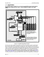
Figure 17
shows the ETU and CLK control circuits. The
firmware determines when clock stop is supported by the smart card and when it is appropriate to go into
that mode (and when to come out of it). The smart card UART is clocked by the same clock that is
provided to the selected smart card. The transition between smart card clocks is handled in hardware to
eliminate any glitches for the UART during switchover. The external smart card clock is not affected
when switching the UART to communicate with the internal smart card.
72
Rev.
1.2


