EDM1-IMX6PLUS HARDWARE MANUAL
– VER 1.00 – NOV 16 2016
Page
22
of
83
2.4. NAND Flash Storage
The EDM1-IMX6PLUS can be ordered with onboard NAND Flash storage in different configurations and
capacity.
The following NAND Flash chips have been validated and tested on the EDM1-IMX6PLUS System-on-
Module:
Samsung K9FxG08U0B
More information can be retrieved from your TechNexion sales representative.
Table 4 - NAND Signal Description
i.MX6
BALL
PAD NAME
Signal
V
I/O
Description
A18
NANDF_D0
NAND_DATA00
3V3
I/O
GPMC data bit 0
C17
NANDF_D1
NAND_DATA01
3V3
I/O
GPMC data bit 1
F16
NANDF_D2
NAND_DATA02
3V3
I/O
GPMC data bit 2
D17
NANDF_D3
NAND_DATA03
3V3
I/O
GPMC data bit 3
A19
NANDF_D4
NAND_DATA04
3V3
I/O
GPMC data bit 4
B18
NANDF_D5
NAND_DATA05
3V3
I/O
GPMC data bit 5
E17
NANDF_D6
NAND_DATA06
3V3
I/O
GPMC data bit 6
C18
NANDF_D7
NAND_DATA07
3V3
I/O
GPMC data bit 7
B16
NANDF_RB0
NAND_READY_B 3V3
I
External indication of wait
B17
SD4_CMD
NAND_RE_B
3V3
O
GPMC Read Enable
F15
NANDF_CS0
NAND_CE0_B
3V3
I/O
GPMC Chip Select 0
C15
NANDF_CLE
NAND_CLE
3V3
O
GPMC Lower Byte Enable. Also used for
Command Latch Enable
A16
NANDF_ALE
NAND_ALE
3V3
O
GPMC Address Valid or Address Latch
Enable
E16
SD4_CLK
NAND_WE_B
3V3
I
GPMC Write Enable
E15
NANDF_WP_B
NAND_WP_B
3V3
O
GPMC Write Protect / Enable
NOTE: On configurations where NAND Flash is mounted instead of eMMC, EDM PIN# 86 is not
connected.
Summary of Contents for EDM1-IMX6PLUS
Page 1: ...EDM1 IMX6PLUS VER 1 00 November 16 2016 ...
Page 21: ...EDM1 IMX6PLUS HARDWARE MANUAL VER 1 00 NOV 16 2016 Page 21 of 83 Figure 8 eMMC Schematics ...
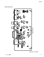
Page 23: ...EDM1 IMX6PLUS HARDWARE MANUAL VER 1 00 NOV 16 2016 Page 23 of 83 Figure 9 NAND IC Schematics ...
Page 27: ...EDM1 IMX6PLUS HARDWARE MANUAL VER 1 00 NOV 16 2016 Page 27 of 83 Figure 11 WiFi BT Schematics ...