Design Considerations
21
• ESD protection devices are recommended for applications which are subject to external
contact. The restrictions with regard to capacitive loading have to be applied when
selecting a protection device.
The USB specification (revision 2.0 of April 27, 2000, chapter 7.1.1.1) demands a
cable with a characteristic impedance of 90 Ω ± 15%. Matching this impedance would
require a driver output impedance of 45 Ω on both the negative and the positive driver.
Nevertheless, the controller demands external resistors of 27 Ω. These would correspond
to intrinsic resistances of the drivers of 18 Ω.
The USB specification demands a switchable pull-up resistor of 1.5 kΩ on USB-
which identifies the UDP as a full speed device to the attached host controller. On this
module, this resistor is integrated on the chip. It can be switched on or off using the "USB
Pad Pull-up Control Register", which is part of the "Bus Matrix User Interface" (not the
"USB Device Port User Interface", as one might expect). This pull-up resistor is required
to be switchable in order not to source current to an attached but powered down host.
This would otherwise constitute an irregular condition on the host. The software has to
take care of this fact.
The capacitors are intended to improve the signal quality (edge rate control) in
dependency of the specific design. They are not mandatory. The total capacitance to
ground of each USB pin, the PCB trace to the series resistor, and the capacitor must not
exceed 75pF.
Operation with V
BUS
as a Supply.
Special care has to be taken if the module is
powered by the VBUS supply. Please refer to the appropriate rules in the USB specification
with regard to inrush current limiting and power switching. As the module draws more
than 100mA in normal mode, it is a "high-power" device according to the specification
(<100mA = "low-power", 100..500mA = "high-power"). It therefore requires staged
switching which means that at power-up it should draw not more than 100mA on VBUS.
The capacitive load of a USB device on VBUS should be not higher than 10µF.
Layout considerations.
The external resistors should be placed in the vicinity of the
module's connector. The traces of the differential pair (USB- and USB-Device- )
should not encircle large areas on the base board, in order to reduce signal distortion and
noise. The are preferably routed closely in parallel to the USB connector.
5.3. Ethernet Controller
Please take care of the specific layout requirements of the Ethernet port when designing
a base board. The two signals of the transmitter pair (ETX+ and ETX-) should be routed
in parallel (constant distance, e.g. 0.5mm) with no vias on their way to the RJ45-jack. The
same is true for the receiver pair (ERX+ and ERX-). No other signals should be crossing
or get next to these lines. If a ground plane is used on the base board, it should be omitted
in the vicinity of the Ethernet signals.
A 1nF / 2kV capacitor should be connected between board ground and chassis ground
(which is usually connected to the shield of the RJ45-jack).
Two LED outputs from the DM9000A controller can be used on the base board. LED_S
indicates the current speed of the Ethernet connection (100MBit = on, 10 MBit = off).
Summary of Contents for Panel-Card
Page 1: ...Panel Card Technical Reference ...
Page 32: ...Panel Card Starterkit 26 Figure 6 1 Panel Card EVB Schematics Bus JTAG ...
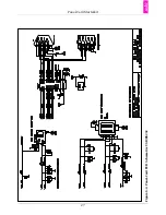
Page 33: ...Panel Card Starterkit 27 Figure 6 2 Panel Card EVB Schematics USB RS232 ...
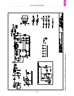
Page 34: ...Panel Card Starterkit 28 Figure 6 3 Panel Card EVB Schematics Power Regulation ...
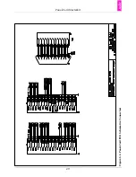
Page 35: ...Panel Card Starterkit 29 Figure 6 4 Panel Card EVB Schematics Connectors ...
Page 36: ...Panel Card Starterkit 30 Figure 6 5 Panel Card EVB Schematics HID ...
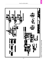
Page 39: ...Panel Card Starterkit 33 Figure 6 8 Panel Card Connector Schematics USB Ethernet ...
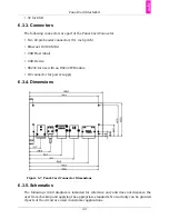
Page 49: ...Panel Card Dimensions 43 Appendix H Panel Card Dimensions Figure H 1 Panel Card 35 Dimensions ...
Page 50: ...Panel Card Dimensions 44 Figure H 2 Panel Card 57 Dimensions ...


