


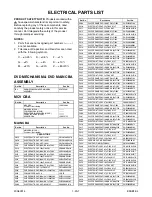
1-15-5
W3N4HTI
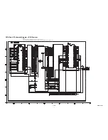
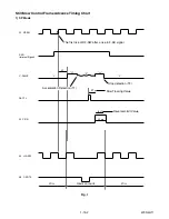
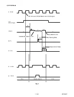
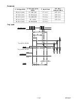
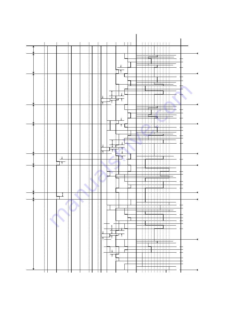
Fig. 4
PIN NO
.
LD-SW
CL/SS
LM-FWD "M"
/REV
C-DRIVE
"Z"
ON
ON
C-F/R
DR
UM
R
O
T
A
TION
P-ON-L
A-MUTE-H
D-REC-H
D-PB
EJ
AU
RS
SF
SM
TL
FB
AL
SB
87
26
32
27
31
29
TV/VIDEO
9
DISPLA
Y
ST-S/
END-S
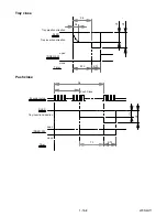
"ON"
REC
REW
FF
STOP
/EJECT
0.5S
1.0S
0.2S
0.5S
0.2S
0.5S
0.5S
0.5S
0.2S
0.2S
0.2S
1.5S
2.5S Short REV
1.0S
0.2S
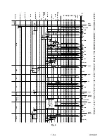
LD-FWD
REV
LD-FWD
STOP(A)
STOP(A)
STOP(A)
CASS. UNLD
EJECT
STOP(A)
LD-REV
FF
LD-REV
LD-REV
LD-FWD
LD-FWD
LD-FWD
LD-FWD
LD-FWD
LD-FWD
LD-FWD
REC PAUSE
REC
REC
REW
LD-REV
LD-REV
LD-REV
LD-REV
LD-REV
LD-REV
LD-REV
PAUSE
REC or
PAUSE
STOP
/EJECT
STOP
/EJECT
STOP
/EJECT
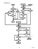
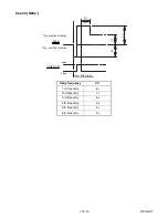
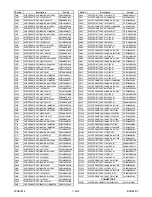
2.
ST
OP(A) -> FF -> ST
OP(A) -> REW -> ST
OP(A) -> REC -> P
A
USE -> P
A
USE or REC -> ST
OP(A) -> EJECT
ST
OP
FF
STOP
REW
ST
OP
REC
REC
REC P
A
USE
ST
OP
TL
TL
SM
SM
SF
SF
AL
AL
SM
AL
AL
AL
AU
AU
SM
TL
SB
EJ
RS
RS
SM
SM
SF
FB
SM
A
U
A
U
SS
SS
SS
SF
AU
AL
AL
A
U
SS
FB
CL
SF
FB
SM
FB
SF
A
U
A
U
FB
SF
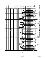
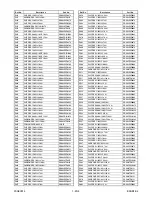
1.0S
1.2S
0.2S
0.2S
40mS
0.4S
0.2S
0.2S
0.4S
20mS
40mS
0.2S
20mS
0.2S
0.4S
40mS
20mS
0.1S
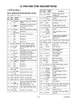
Summary of Contents for CWV20V6
Page 37: ...1 12 3 Main 1 7 Schematic Diagram VCR Section E9AB1SCM1...
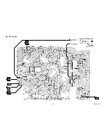
Page 38: ...1 12 4 Main 2 7 Power SW DVD Open Close SW Sensor Schematic Diagram VCR Section E9AB1SCM2...
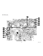
Page 39: ...1 12 5 Main 3 7 Schematic Diagram VCR Section E9AB1SCM3...
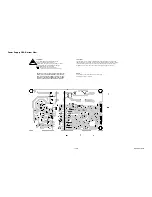
Page 40: ...1 12 6 Main 4 7 Schematic Diagram VCR Section E9AB1SCM4...
Page 41: ...1 12 7 Main 5 7 Schematic Diagram VCR Section E9AB1SCM5...
Page 42: ...1 12 8 Main 6 7 Schematic Diagram VCR Section E9AB1SCM6...
Page 43: ...1 12 9 Main 7 7 Schematic Diagram VCR Section E9AB1SCM7...
Page 45: ...1 12 11 Front Jack Schematic Diagram VCR Section E9AB1SCJK...
Page 82: ...CWV20V6 E9AB1CD 2006 10 6...


