


1-4-3
DVDN_SN
With Iron Wire:
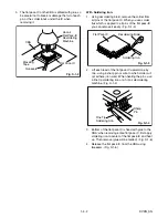
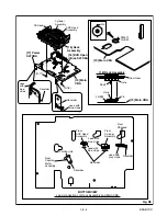
1. Using desoldering braid, remove the solder from
all pins of the flat pack-IC. When you use solder
flux which is applied to all pins of the flat pack-IC,
you can remove it easily. (Fig. S-1-3)
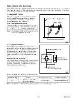
2. Affix the wire to a workbench or solid mounting
point, as shown in Fig. S-1-5.
3. While heating the pins using a fine tip soldering
iron or hot air blower, pull up the wire as the solder
melts so as to lift the IC leads from the CBA
contact pads as shown in Fig. S-1-5.
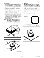
4. Bottom of the flat pack-IC is fixed with glue to the
CBA; when removing entire flat pack-IC, first apply
soldering iron to center of the flat pack-IC and heat
up. Then remove (glue will be melted). (Fig. S-1-6)
5. Release the flat pack-IC from the CBA using
tweezers. (Fig. S-1-6)
Note:
When using a soldering iron, care must be
taken to ensure that the flat pack-IC is not
being held by glue. When the flat pack-IC is
removed from the CBA, handle it gently
because it may be damaged if force is applied.
2. Installation
1. Using desoldering braid, remove the solder from
the foil of each pin of the flat pack-IC on the CBA
so you can install a replacement flat pack-IC more
easily.
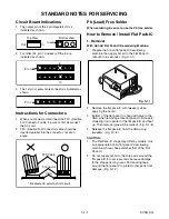
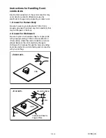
2. The “
●
” mark on the flat pack-IC indicates pin 1.
(See Fig. S-1-7.) Be sure this mark matches the 1
on the PCB when positioning for installation. Then
presolder the four corners of the flat pack-IC. (See
Fig. S-1-8.)
3. Solder all pins of the flat pack-IC. Be sure that
none of the pins have solder bridges.
To Solid
Mounting Point
Soldering Iron
Iron Wire
or
Hot Air Blower
Fig. S-1-5
Fine Tip
Soldering Iron
CBA
Flat Pack-IC
Tweezers
Fig. S-1-6
Example :
Pin 1 of the Flat Pack-IC
is indicated by a " " mark.
Fig. S-1-7
Presolder
CBA
Flat Pack-IC
Fig. S-1-8
Summary of Contents for CWV20V6
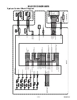
Page 37: ...1 12 3 Main 1 7 Schematic Diagram VCR Section E9AB1SCM1...
Page 38: ...1 12 4 Main 2 7 Power SW DVD Open Close SW Sensor Schematic Diagram VCR Section E9AB1SCM2...
Page 39: ...1 12 5 Main 3 7 Schematic Diagram VCR Section E9AB1SCM3...
Page 40: ...1 12 6 Main 4 7 Schematic Diagram VCR Section E9AB1SCM4...
Page 41: ...1 12 7 Main 5 7 Schematic Diagram VCR Section E9AB1SCM5...
Page 42: ...1 12 8 Main 6 7 Schematic Diagram VCR Section E9AB1SCM6...
Page 43: ...1 12 9 Main 7 7 Schematic Diagram VCR Section E9AB1SCM7...
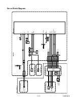
Page 45: ...1 12 11 Front Jack Schematic Diagram VCR Section E9AB1SCJK...
Page 82: ...CWV20V6 E9AB1CD 2006 10 6...