Electrical characteristics
STM32F038x6
68/102
DocID026079 Rev 3
6.3.14
NRST and NPOR pin characteristics
NRST pin characteristics
The NRST pin input driver uses the CMOS technology. It is connected to a permanent pull-
up resistor, R
PU
.
Unless otherwise specified, the parameters given in the table below are derived from tests
performed under the ambient temperature and supply voltage conditions summarized in
Table 18: General operating conditions
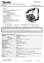
Figure 22. Recommended NRST pin protection
1. The external capacitor protects the device against parasitic resets.
2. The user must ensure that the level on the NRST pin can go below the V
IL(NRST)
max level specified in
Table 47: NRST pin characteristics
. Otherwise the reset will not be taken into account by the device.
NPOR pin characteristics
The NPOR pin input driver uses the CMOS technology. It is connected to a permanent pull-
up resistor to the V
DDA
, R
PU
.
Unless otherwise specified, the parameters given in
below are derived from tests
performed under ambient temperature and supply voltage conditions summarized in
Table 18: General operating conditions
Table 47. NRST pin characteristics
Symbol
Parameter
Conditions
Min
Typ
Max
Unit
V
IL(NRST)
NRST input low level voltage
-
-
-
0.3 V
DD
+0.07
(1)
V
V
IH(NRST)
NRST input high level voltage
-
0.445 V
DD
+0.398
-
-
V
hys(NRST)
NRST Schmitt trigger voltage
hysteresis
-
-
200
-
mV
R
PU
Weak pull-up equivalent
resistor
(2)
V
IN
=
V
SS
25
40
55
k
Ω
V
F(NRST)
NRST input filtered pulse
-
-
-
100
ns
V
NF(NRST)
NRST input not filtered pulse
-
700
-
-
ns
1. Data based on design simulation only. Not tested in production.
2. The pull-up is designed with a true resistance in series with a switchable PMOS. This PMOS contribution to the series
resistance is minimal (~10% order).
5
38
9
''
,QWHUQDOUHVHW
([WHUQDO
UHVHWFLUFXLW
1567
)LOWHU
)
069