STR-DG820
64
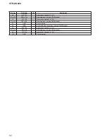
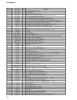
Pin No.
Pin Name
I/O
Description
D11
ACLKX2
O
Interruput signal output to the system controller
D12, D13
DVDD
-
Power supply terminal (+3.3V) (for IO)
D14
EM_WAIT
I
Not used
D15
EM_OE#
O
Not used
D16
SPI0_ENA#
I
Chip enable signal input from the system controller
E1
ACLKR1
I
Bit clock signal input from the digital audio interface receiver and HDMI receiver
E2
ACLKX1
O
Bit clock signal output to the D/A converter
E3
UHPI_HD[21]
I/O
Not used
E4
DVDD
-
Power supply terminal (+3.3V) (for IO)
E5
VSS
-
Ground terminal
E6 to E11
CVDD
-
Power supply terminal (+1.26V) (for core)
E12
VSS
-
Ground terminal
E13
DVDD
-
Power supply terminal (+3.3V) (for IO)
E14
UHPI_HD[18]
I/O
Not used
E15
EM_CS[2]#
O
Not used
E16
EM_RW
O
Not used
F1
AFSR1
I
L/R sampling clock signal input from the digital audio interface receiver and HDMI receiver
F2
AFSX1
O
L/R sampling clock signal output to the D/A converter
F3, F4
UHPI_HD[19],
UHPI_HD[20]
I/O
Not used
F5 to F12
VSS
-
Ground terminal
F13, F14
UHPI_HD[10],
UHPI_HD[9]
I/O
Not used
F15
EM_CS[0]#
O
Chip select signal output to the SD-RAM
F16
EM_RAS#
O
Row address strobe signal output to the SD-RAM
G1
VSS
-
Ground terminal
G2
RESET#
I
Reset signal input from the system controller "L": reset
G3, G4
UHPI_HD[17],
UHPI_HD[18]
I/O
Not used
G5
CVDD
-
Power supply terminal (+1.26V) (for core)
G6 to G11
VSS
-
Ground terminal
G12
CVDD
-
Power supply terminal (+1.26V) (for core)
G13, G14
UHPI_HD[12],
UHPI_HD[11]
I/O
Not used
G15
EM_BA[0]
O
Bank address signal output to the SD-RAM
G16
VSS
-
Ground terminal
H1
UHPI_HD[16]
I/O
Not used
H2
CLKIN
I
Not used
H3
VSS
-
Ground terminal
H4
UHPI_HD[31]
I/O
Not used
H5
CVDD
-
Power supply terminal (+1.26V) (for core)
H6 to H11
VSS
-
Ground terminal
H12
CVDD
-
Power supply terminal (+1.26V) (for core)
H13, H14
UHPI_HD[14],
UHPI_HD[13]
I/O
Not used
H15
EM_A[10]
O
Address signal output to the SD-RAM
H16
EM_BA[1]
O
Bank address signal output to the SD-RAM
J1
OSCVSS
-
Ground terminal for oscillator
J2
OSCIN
I
System clock input terminal (25 MHz)
J3
OSCOUT
O
System clock output terminal (25 MHz)
J4
OSCVDD
-
Power supply terminal for oscillator
J5
CVDD
-
Power supply terminal (+1.26V) (for core)
J6 to J11
VSS
-
Ground terminal
J12
CVDD
-
Power supply terminal (+1.26V) (for core)
J13
UHPI_HD[15]
I/O
Not used
J14
DVDD
-
Power supply terminal (+3.3V) (for IO)
J15, J16
EM_A[1], EM_A[0]
O
Address signal output to the SD-RAM
Summary of Contents for STRDG820 - STR AV Receiver
Page 95: ...MEMO STR DG820 95 ...

