STR-DG820
66
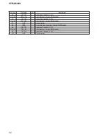
Pin No.
Pin Name
I/O
Description
R5 to R13
EM_D[6], EM_D[4],
EM_D[2], EM_D[1],
EM_D[15], EM_D[13],
EM_D[12], EM_D[10],
EM_D[8]
I/O
Two-way data bus with the SD-RAM
R14
EM_CLK
O
Clock signal output to the SD-RAM
R15
EM_DQM[3]
O
Byte enable signal output to the SD-RAM
R16
DVDD
-
Power supply terminal (+3.3V) (for IO)
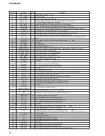
T1
VSS
-
Ground terminal
T2
DVDD
-
Power supply terminal (+3.3V) (for IO)
T3
EM_WE#
O
Write enable signal output to the SD-RAM
T4 to T6
EM_D[7], EM_D[5],
EM_D[3]
I/O
Two-way data bus with the SD-RAM
T7
VSS
-
Ground terminal
T8, T9
EM_D[0], EM_D[14]
I/O
Two-way data bus with the SD-RAM
T10
VSS
-
Ground terminal
T11, T12
EM_D[11], EM_D[9]
I/O
Two-way data bus with the SD-RAM
T13
EM_DQM[1]
O
Byte enable signal output to the SD-RAM
T14
EM_CKE
O
Clock enable signal output to the SD-RAM
T15
DVDD
-
Power supply terminal (+3.3V) (for IO)
T16
VSS
-
Ground terminal
Summary of Contents for STRDG820 - STR AV Receiver
Page 95: ...MEMO STR DG820 95 ...


