


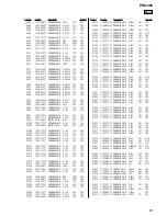


41
PRS-500
Pin No.
Pin Name
I/O
Description
D4
VDD
—
+3V0
D5
VDD
—
+3V0
D6
VSS
—
Ground
D7
VSS
—
Ground
D8
n.c.
—
Not used (Open)
D9
VSS
—
Ground
D10
VSS
—
Ground
D11
VDD
—
+3V0
D12
VSS
—
Ground
D13
VDD
—
+3V0
D14
SRC_OE
O
Output enable for source driver
D15
GT_SPV
O
Start signal for gate driver
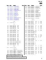
E1
A4
O
22 bits address bus
E2
A5
O
22 bits address bus
E3
D16
I/O
32 bits data bus
E4
VSS
—
Ground
E5
n.c.
—
Not used (Open)
E12
VSS
—
Ground
E13
SRC_CL
O
Clock for source driver
E14
GT_MODE
O
Mode select for gate driver
E15
GT_CKV
O
Clock for gete driver
F1
A6
O
22 bits address bus
F2
A7
O
22 bits address bus
F3
F_NOE
O
Output enable for Flash
F4
VSS
—
Ground
F12
n.c.
—
Not used (Open)
F13
TST0
I
Test mode (normal = “0”)(Not used (Fixed to “L”))
F14
GT_CASC
O
CAS select for gate driver
F15
H_NRST
I
Reset from main CPU
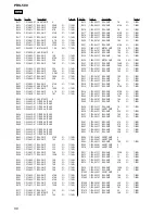
G1
A8
O
22 bits address bus
G2
A9
O
22 bits address bus
G3
A10
O
22 bits address bus
G4
VSS
—
Ground
G12
VSS
—
Ground
G13
VDD
—
+3V0
G14
H_CD
I
Command/Data from main CPU
G15
H_WUP
I
Wakeup from main CPU
H1
A12
O
22 bits address bus
H2
A11
O
22 bits address bus
H3
VDD
—
+3V0
H4
n.c.
—
Not used (Open)
H12
n.c.
—
Not used (Open)
H13
VDD
—
+3V0
H14
H_D7
I/O
8 bits data bus for main CPU
H15
H_D6
I/O
8 bits data bus for main CPU
J1
A14
O
22 bits address bus
J2
A13
O
22 bits address bus
J3
A18
O
22 bits address bus
J4
VSS
—
Ground


