


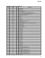

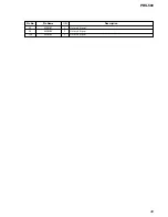

35
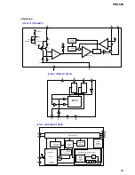
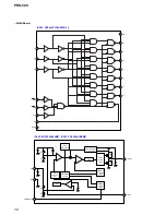
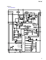
PRS-500
Pin No.
Pin Name
I/O
Description
G7
NVDD4
—
2.9V DC input
G8
NVSS
—
Ground
G9
NVSS
—
Ground
G10
QVSS
—
Ground
G11
PA2
—
Not used (Open)
G12
ED3
I/O
8 bits data bus for indicator
G13
ED7
I/O
8 bits data bus for indicator
G14
DSPSIOEN
—
Not used (Open)
G15
ED5
I/O
8 bits data bus for indicator
H1
A15
O
25 bits address bus
H2
A16
O
25 bits address bus
H3
D23
I/O
32 bits data bus
H4
D24
I/O
32 bits data bus
H5
D22
I/O
32 bits data bus
H6
NVSS
—
Ground
H7
NVSS
—
Ground
H8
NVSS
—
Ground
H9
NVSS
—
Ground
H10
NVDD2
—
2.9V DC input
H11
ED1
I/O
8 bits data bus for indicator
H12
PCSD
O
Suspend output for SD controller
H13
PCM
—
Not used (Open)
H14
AUDIO1
O
Chip select output for DAC
H15
TMS
I
Test mode select input for test (Not used (Fixed to “H”))
J1
A14
O
25 bits address bus
J2
A12
O
25 bits address bus
J3
D21
I/O
32 bits data bus
J4
D20
I/O
32 bits data bus
J5
NVDD1
—
2.9V DC input
J6
NVSS
—
Ground
J7
NVSS
—
Ground
J8
QVDD1
—
1.95V DC input
J9
NVSS
—
Ground
J10
ED6
I/O
8 bits data bus for indicator
J11
AUDIO2
O
Command clock output for DAC
J12
TCK
I
Test clock input for test (Not used (Fixed to “H”))
J13
TDO
O
Serial data output for test (Not used (Fixed to “H”))
J14
BOOT1
I
System boot mode select input (Pull
-
down) (Not used (Fixed to “L”))
J15
BOOT0
I
System boot mode select input (Pull
-
up) (Not used (Fixed to “H”))
K1
A13
O
25 bits address bus
K2
A11
O
25 bits address bus
K3
CS2
O
Chip select
K4
D19
I/O
32 bits data bus
K5
NVDD1
—
2.9V DC input
K6
NVSS
—
Ground
K7
QVSS
—
Ground
K8
NVDD1
—
2.9V DC input
K9
NVSS
—
Ground
K10
D1
I/O
32 bits data bus