background image

– 15 –

KP-44PX2/44PX2U

RM-938

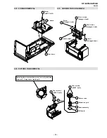
3-1.

REAR  BOARD  REMOVAL

3-3.

SERVICE  POSITION

3-2.

MAIN  BRACKET  BLOCK  REMOVAL

SECTION 3  DISASSEMBLY

3-4.

FRONT  PANEL  REMOVAL

Rear board

Twelve screws

(Hexagon head)

      Two screws

(Hexagon head)

1

2

Main bracket block

Light shield

     board

1

2

3

Main bracket block

1

1

2

Front Panel

Two screws

(Hexagon head)

Summary of Contents for KP-44PX2

Page 1: ...KP 44PX2 44PX2U RM 938 SERVICEMANUAL AE 6XCHASSIS MODEL COMMANDER DEST CHASSIS NO KP 44PX2 RM 938 AEP SCC Q85C A MODEL COMMANDER DEST CHASSIS NO PROJECTION TV RM 938 KP 44PX2U RM 938 UK SCC Q84G A KP 44PX2 ...

Page 2: ...t 31 6 4 White Balance Adjustment 31 6 5 Sub Bright Adjustment 31 6 6 Sub Color Adjustment 31 6 7 Auto Convergence Error Code List 32 6 8 Test Test Mode 33 7 DIAGRAMS 7 1 Block Diagrams 35 7 2 Circuit Boards Location 40 7 3 Schematic Diagrams and Printed Wiring Boards 40 A Board Schematic Diagram 1 2 41 A Board Schematic Diagram 2 2 42 A Printed Wiring Board 43 AP Board Schematic Diagram 45 AP Pri...

Page 3: ...n o C t u p t u O s l a n g i S s e r u t a e F r e h t O e s i o N o t u A R N D F C D s u l P l a t i g i D z H 0 0 1 e z e e r F e r u t c i P t x e t e l e T P I P n o i t c u d e R P S D E B B y b l o D l a u t r i V E D I S s l a n i m r e T t u p t u O t u p n I l o r t n o C d e r a r f n I m e t s y S l o r t n o C e t o m e R k c a j e n o h p d a e H k c a j i n i m o e r e t s s t n e ...

Page 4: ...sitive 12 Open 13 Ground red 14 Ground blanking 15 _ _ Red input 0 7 3dB 75 ohms positive _ S signal Chroma input 0 3 3dB 75 ohms positive 16 Blanking input Ys signal High state 1 3V Low state 0 0 4V Input impedence 75 ohms 17 Ground video output 18 Ground video input 19 Video output 1V 3dB 75ohms positive sync 0 3V 3 10dB 20 _ _ Video input 1V 3dB 75ohms positive sync 0 3V 3 10dB _ Video input Y ...

Page 5: ...E d n e k c a B 4 1 r o r r E e c n e g r e v n o C c i m a n y D 5 1 r o r r E P I P 6 1 Table 1 How to enter intoTable 2 1 Turn on the main power switch of the TV set 2 Program Remote Commander for Operation in Service Mode See Page 23 3 Press VIDEO VIDEO MENU on the Remote Commander 4 Using the Remote Commander Scroll to the Error Menu item using the down arrow key then press the right arrow ke...

Page 6: ... screen 2 Press the or button on the remote control to select the language then press the OK button to confirm your selection From now on all the menus will appear in the selected language 3 The Country menu appears automatically on the TV screen Press the or button to select the country in which you will operate the TV set then press the OK button to confirm your selection If the country in which...

Page 7: ...ction Sound Adjustment on page 12 Refer to the section RGB Centring on page 17 Menu System Refer to the section Sleep Timer on page 13 Refer to the section Auto Format on page 13 Refer to the section AV3 Output on page 13 Refer to the section PIP Input on page 14 Refer to the section PIP Position on page 14 Refer to the section Language Country on page 14 Refer to the section Auto Tuning on page 1...

Page 8: ... Noise Reduction Personal AUTO Sound Adjustment Select Enter Menu Effect Treble Bass Balance Reset Dual Sound Auto Volume TV Speakers Natural Off Stereo On Sound Adjustment Select Enter Effect Treble Bass Balance Reset Dual Sound Auto Volume TV Speakers Natural Off Stereo On 13 GB Menu System Level 1 Level 2 Level 3 Function SLEEP TIMER The Sleep Timer option in the Features menu allows you to sel...

Page 9: ...u to change the order in which the channels TV Broadcast appear on the screen To do this after selecting the option press and then proceed in the same way as in step 6 b of the section Switching On the Projection TV and Automatically Tuning on page 9 PROGRAMME LABELS The Programme Labels option in the Set Up menu allows you to name a channel using up to five characters letters or numbers To do thi...

Page 10: ...o this highlighting the Programme option press the PROG button to select the programme number you want to skip When the programme you want to skip appears on the screen select the Skip option and press Next press or to select Yes Finally press OK twice to confirm and store To cancel this function afterwards select No instead of Yes in the step above e View and record scrambled channels when using ...

Page 11: ...watching TV and after more than 50 of NexTView data is available 100 data may not be available depending on the area the indication NexTView coloured black is displayed on the screen Press the button on the remote control to watch the Overview interface see fig 2 As soon as you enter the NexTView service the of NexTView data available will be shown in the bottom left corner of the screen Once you ...

Page 12: ...gs can be modified through the Sound Adjustment menu To enjoy Dolby Virtual sound effect through your Hi Fi equipment Place the speakers of your equipment in front of your listening position and beside the projection TV set but keeping a distance of 50 cm between each speaker and the projection TV set Then by using the menu system select the menu Sound Adjustment Next select Dolby V on the Effect ...

Page 13: ...or try the next code listed against the brand Your brand codes may be lost if weak batteries are not replaced within a few minutes To reset your brand of DVD or VCR please repeat the above steps A small label is added inside the battery door to allow you to record your brand codes Not all brands are covered and not all models of every brand may be covered Additional Information 2 1 3 VCR Brand Lis...

Page 14: ...characters appear when viewing teletext Wrong characters appear when viewing NexTView Brightness level of the picture is notoriously decreased when viewing a teletext page Remote control does not function The standby indicator on the projection TV flashes S Solution Check the aerial connection Plug the TV in and press the button on the front of the projection TV If the standby indicator is on pres...

Page 15: ...ICE POSITION 3 2 MAIN BRACKET BLOCK REMOVAL SECTION 3 DISASSEMBLY 3 4 FRONT PANEL REMOVAL Rear board Twelve screws Hexagon head Two screws Hexagon head 1 2 Main bracket block Light shield board 1 2 3 Main bracket block 1 1 2 Front Panel Two screws Hexagon head ...

Page 16: ...X2 44PX2U RM 938 3 5 RESISTOR ASSEMBLY FOCUS PACK REMOVAL 3 6 H1 AND H3 BOARD REMOVAL 2 Screw BVTP 4x16 4 3 1 Four screws Hexagon head Front board Resistor assembly Focus pack 3 2 1 H3 board Front panel H1 board ...

Page 17: ...Eleven screws BVTP 4x16 Four screws Hexagon head 1 2 3 5 4 Three claws Six screws BVTP 3x12 Screw BVTP 3x12 Screw BVTP 3x12 Printed circuit board support 4 6 AP board Claw 7 D board 3 8 HIGH VOLTAGE CABLE REMOVAL AND INSTALLATION 1 2 1 2 1 Removal 2 Installation 3 4 Rubber cap Rubber cap HV cable turn 90 HV cable Hook Gutter ...

Page 18: ... 18 KP 44PX2 44PX2U RM 938 3 10 TERMINAL BOARD REMOVAL 3 11 G BOARD REMOVAL 1 2 G board Five claws 2 1 Terminal board Six screws BVTP 4x16 ...

Page 19: ... screws BTVP 4x16 5 7 Removing the arrow marked screw is strictly inhibited If removed it may cause liquid spill Four screws BTVP 4x16 Lens CR board Neck assembly Deflection yolk Picture tube 3 13 CHASSIS BLOCK REMOVAL 3 Screw Hexagon head 4 3 1 2 Screw Hexagon head Two screws Hexagon head Three screws Hexagon head Chassis block ...

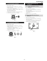
Page 20: ...oke Anode cap R G SCREEN B R G FOCUS Focus Pack B Fig 4 4 Lens Fig 4 3 Fig 4 2 Test signal Minimize both A and B A B 5 Rotate the green lens and align to obtain the best lens focus at the center area 6 Rotate the green focus VR on the focus pack and align to obtain the best electrical focus in the top right corner 7 Perform the same alignment for red and blue lenses and electric focus 8 Fix lens s...

Page 21: ...et to under focus to enlarge the spot 4 Now align the 4 Pole Magnet so that the enlarged spot becomes a perfect circle 5 Perform the same alignment for red and blue Fig 4 7 Fig 4 8 Adjust Point Use the center dot Use the center dot OK NG NG 4 7 GREEN RED AND BLUE FOCUS ADJUSTMENT 4 7 1 Green Red and Blue Lens Focus Adjustment 1 Receive the Monoscope signal 2 Place the caps on the red and blue lens...

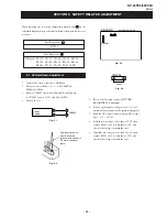
Page 22: ...01 5 Receive the Dot signal and set PICTURE BRIGHTNESS to minimum 6 Slowly up the supply voltage from 0 V to 135 V until hold down circuit works picture disappear 7 Read the HV static voltmeter of peak HV voltage Spec 33 7 35 3 kV 8 If Hold down voltage is less than 33 7 kV then replace R9901 of 43 k with that of 39 k and check if the voltage is within the spec 9 If hold down voltage is over than ...

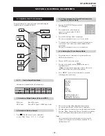
Page 23: ... on the remote commander to obtain the following menu on the screen 5 Move to the corresponding adjustment item using the up or down arrow buttons on the Remote Commander 6 Press the right arrow button to enter into the required menu item 7 Press the Menu button on the Remote Commander to quit the Service Mode when all adjustments have been completed Note After carrying out the service adjustments...

Page 24: ... 1 1 5 0 1 3 0 1 1 5 0 1 3 0 1 1 5 0 1 3 0 1 1 5 0 1 1 5 0 3 2 0 1 0 3 2 0 1 0 7 4 0 2 0 7 4 0 2 0 7 4 0 2 0 7 4 0 2 0 5 1 0 7 0 7 0 7 0 7 0 7 0 7 0 3 0 1 0 0 0 0 0 1 2 3 0 2 3 0 4 0 0 2 6 0 0 2 9 4 9 2 7 4 0 4 8 3 1 0 9 1 6 7 0 0 0 0 0 0 0 0 0 0 0 0 0 6 9 9 2 0 3 3 5 6 7 4 1 D N U O S N M D M S M M S M D M N E B B 1 B 2 B 3 B 4 B 5 B L W S F W S D A C M A C I N r o r r E M A C I N o e r e t S 1 1...

Page 25: ...h of BLUE vertical clamp 31 RHCS Start position of RED horizontal clamp 32 RHCW Width of RED horizontal clamp 33 GHCS Start position of GREEN horizontal clamp 34 GHCW Width of GREEN horizontal clamp 35 BHCS Start position of BLUE horizontal clamp 36 BHCW Width of BLUE horizontal clamp 37 BDVU 23 18 27 21 23 18 27 21 Vertical position for border line 1 38 BDVL 905 686 1061 811 905 686 1061 811 Vert...

Page 26: ...tal Vertical size LIN GREEN Horizontal Vertical linearity KEY GREEN Vertical keystone PIN GREEN Horizontal Vertical pincushion MLIN GREEN Horizontal mid linearity MSIZ GREEN Horizontal mid size CENT BLUE Horizontal Vertical center SKEW BLUE Horizontal Vertical skew SIZE BLUE Horizontal Vertical size LIN BLUE Horizontal Vertical linearity KEY BLUE Vertical keystone PIN BLUE Horizontal Vertical pinc...

Page 27: ... 2 Main Deflection Adjustment The data values are same in all modes and therefore the adjustment for the PAL Wide mode only is performed here 1 Place the caps on the red and blue lenses so that only the green color is displayed 2 Enter the PAL SPCB signal and set the TV to PAL mode 3 Set the screen format to Wide 4 Program the remote commander for operation in Service Mode and enter Service Menu S...

Page 28: ...a 3 Select GRN CENT When BLU or RED is displayed press 3 button on the commander to change the adjustment color in the order of GRN c BLU c RED 4 In the GRN BLU or RED mode v V keys on the joystick can change the data in vertical direction or b B keys in horizontal direction 5 Before returning to the Service menu press MUTE 0 buttons on the commander to write the data Omission of this operation ca...

Page 29: ... b B keys on the joystick 6 Press 9 button on the commander to return to the rough adjustment mode CROSSHATCH Movement when v key on joystick is pressed Movement when B key on joystick is pressed CROSSHATCH 6 2 4 Projector Engine Adjustment Sub Deflection Adjustment Push the joystick to v Push the joystick to V Push the joystick to B Push the joystick to b GRN CENT horizontally vertically Adjustme...

Page 30: ...een are symmetrical left and right 10 Select GRN KEY and adjust so that upper and lower horizon tal lines on the screen become parallel GRN KEY vertically GRN PIN horizontally vertically Push the joystick to v Push the joystick to V Push the joystick to B Push the joystick to b Push the joystick to B Push the joystick to b Push the joystick to B Push the joystick to b Push the joystick to B Push t...

Page 31: ...ot 00 recheck Refer to 6 7 7 Exit the TT mode 8 Enter the NTSC monoscope signal and perform the same steps in the NTSC Wide mode respectively a b c Same level 6 4 WHITE BALANCE ADJUSTMENT 1 Enter the monoscope signal 2 Press MENU button on the commander to enter the Picture Adjustment menu 3 Set the Picture Mode to Personal and the screen format to Wide 4 Enter the Service menu See Page 23 and sel...

Page 32: ...d n o c n o i t a r t s i g e r k c e h c d n a a t a d D I M H 1 7 k c e h C 0 4 w o l f r e v o a t a d i g e r T N E C V 1 1 5 r a e n t o n s i e d o m l l a a t a d T N E C V m r i f n o c d n a a t a d D I M V 6 6 k c e h C 1 4 w o l f r e v o a t a d i g e r T N E C H 1 1 5 r a e n t o n s i e d o m l l a a t a d T N E C H m r i f n o c d n a a t a d D I M H 1 7 k c e h C 2 4 w o l f r e v ...

Page 33: ...djustment 15 Rotation coil test 16 Picture level 50 17 No function 18 No function 19 Factory Mode Enable Disable 20 No function 21 Destination ADEKR 22 Destination BL 23 Destination ADEKR 24 Destination U 25 Destination ADEKR 26 Destination BL 27 Destination ADEKR 28 Destination ADEKR 30 No function 31 Auto Shutoff Disable Enable 32 No function 33 No function 34 No function 35 CRT 4 3 16 9 Display...

Page 34: ... 34 KP 44PX2 44PX2U RM 938 MEMO ...

Page 35: ...5 J2000 REAR L REAR R 11 12 13 14 5 17 1 63 10 20 16 45 30 28 26 25 1 3 5 8 1 1 3 5 11 13 17 18 19 20 MICRO VIDEO HP IN L2 FIL VDN OUT VDP OUT HD OUT E W OUT EXTRA PARA VTIM OUT XRAY IN VPROT VM OUT R OUT G OUT B OUT IK IN XRAY V PROT L OUT R OUT CN1502 TO D BOARD CN5016 CN1501 TO D BOARD CN5017 TO CR BOARD CN7101 TO ZG BOARD CN7608 CN7002 CN7001 IK B OUT G OUT R OUT VM V PROT HV PROT P CONT VTIM ...

Page 36: ...7 5 3 1 IC2605 DEF5V RESET IC2603 PJED CPU I AREGI D0 I AREGI D3 0 G I AREGI D2 I AREGI D1 RESET 0 OSC I OSC 0 XLC I EXLC O VSHIFT O HSHIFT I BINT MAIN SDA MAIN SCL 0 DREGI MUTE I VP I VBLK I DREG SDA 0 DREG SDA DREG SCL I EXODD OVF I DREG OVF I DREG BSY I DREG ACK 0 NVM STOP 0 DREGI RST 0 I2C RST 0 RAM CLR 0 NVM WRITE PROT I HP IC2604 DIGITAL REGI RIN GIN BIN YSIN ROUT GOUT BOUT YSOUT DF RHOUT RV...

Page 37: ... 1 3 2 3 1 Q5201 PROT IC5703 2 3 6 5 7 IC5201 2 4 6 7 1 Q5704 5705 DF AMP Q5102 5106 BUFF HOUT DRV Q5104 H OUT Q5710 5711 PROT V V V DEF 1 3 V RET 2 1 Q5706 5707 G2 MUTE 6 5V G2 DF CN5014 CN5001 FOCUS PACK TO CB BOARD J7301 TO CG BOARD J7201 TO CR BOARD J7101 TO CB BOARD CN7304 TO CG BOARD CN7205 TO CR BOARD CN7104 1 2 CN5003 R1 1 R1 2 CN5020 CN5002 TO ZG BOARD CN7607 135V 135V 33V 1 1 135V 135V I...

Page 38: ...1 6302 PROTECT 19 1 IC6004 SWITCHING IC 7 17 2 16 3 1 11 T6003 PFT 14 1 9 T6100 SBT 8 5 6 3 4 Q6304 VOLT G DET 2 1 IC6304 REF VOLTAGE 5 4 IC6302 STBY 5V REG STBY 5V 3 A K REF IN OUT VS RT COM VG H VG L 15 14 18 VD VC2 VB VC1 Q6100 6102 PROTECT IC6007 MAIN SW Q6004 MCM SW STBY 5V RY6000 D6015 RECT 3 2 1 4 1 4 2 3 AC L IN AC N IN 1 4 5 1 AC L OUT AC N OUT CN6006 CN6007 T6002 LFT T6001 LFT F6001 5A C...

Page 39: ...VOLTAGE DET MUTE DRV 12V Q7302 PEAK CN7303 P TO D BOARD CN5006 Q7202 PEAK 3 1 4 Q7408 Q7409 VM AMP CN7401 135V CN7405 1 ZR DY VM DRIVE 12V VM 1 3 CN7403 V DEF V RET Q7401 7405 7410 BUFFER CORE R H RET R H DEF 2 1 CN7404 Q 4 3 RV SUB DEF RV SUB RET RH SUB DEF RH SUB RET R TO D BOARD CN5010 TO D BOARD CN5009 V H SUB V SUB H VM 3 1 4 Q7608 Q7609 VM AMP CN7602 135V ZG DY VM DRIVE 12V VM 1 3 CN7604 V D...

Page 40: ...fety Replace only with the part numbers specified in the parts list Note B bus ZG ZR CR M2 A AP D G CB CG H2 H3 ZB H1 MODE 3 A 7 A 8 A 9 A 10 A 11 A 3 A 4 A 5 A 6 AV LINK IN 97 93 82 81 59 55 48 53 47 32 25 46 24 76 80 17 52 29 2 28 4 13 73 57 58 18 96 6 5 D 2 D 3 D 4 D 5 D 6 A 16 A 17 A 17 LN D 0 D 1 A 14 A 15 40 39 49 27 38 66 65 37 64 36 33 51 8 50 26 23 67 15 85 86 3 87 88 84 83 89 90 92 91 79...

Page 41: ... 41 A B C D E F G H I J K L M N 1 2 3 4 5 6 7 8 9 10 11 O P Q R S T U V W 12 13 14 15 16 A Schematic Video and Audio Processors Audio Output page 1 2 COMPONENTS MARKED AS XX ARE NOT FITTED ON THIS MODEL ...

Page 42: ...Q R S T U V W 12 13 14 15 16 A Schematic Video and Audio Processors Audio Output page 2 2 COMPONENTS MARKED AS XX ARE NOT FITTED ON THIS MODEL A Board Waveforms 5ms div 5ms div 20us div 10us div 1 4 Vp p H 264 mVp p H 272 mVp p H TP1 TP2 TP3 TP4 688 mVp p H TP4 ...

Page 43: ... n i P V s t l o V 0 0 5 2 C I 1 7 1 2 0 0 7 C I 6 1 0 2 0 0 7 C I 0 4 8 4 2 0 7 1 3 1 4 8 4 3 7 1 8 1 7 2 2 4 0 4 0 9 1 9 3 3 4 0 5 3 3 0 2 0 4 4 0 7 0 1 2 1 6 5 4 3 6 8 0 2 2 7 2 6 4 9 8 0 1 0 3 2 8 8 7 4 9 8 1 1 0 4 2 0 8 4 6 2 0 0 7 C I 1 6 3 5 2 3 4 9 4 5 2 2 0 6 2 2 3 0 5 1 4 3 4 4 7 2 2 5 1 5 0 4 8 4 8 2 3 0 2 5 6 5 5 3 9 2 9 4 3 5 8 5 6 4 3 0 3 4 3 4 5 8 5 7 6 7 1 3 6 5 5 5 4 0 8 0 2 3 9 8...

Page 44: ... Q 6 F 2 1 0 7 Q 5 J 2 0 0 2 D 8 B 7 0 0 3 D 6 B 0 0 2 3 C I 3 E 0 1 0 2 Q 7 D 4 1 0 7 Q 6 J 3 0 0 2 D 8 B 8 0 0 3 D 6 B 0 0 2 6 C I 9 H 1 1 0 2 Q 7 E 5 1 0 7 Q 6 I 4 0 0 2 D 7 B 9 0 0 3 D 6 B 1 0 2 6 C I 0 1 H 0 0 5 2 Q 7 F 7 1 0 7 Q 6 I 5 0 0 2 D 5 B 1 1 0 3 D 4 B 2 0 2 6 C I 5 F 1 0 5 2 Q 7 E 8 1 0 7 Q 5 I 6 0 0 2 D 6 B 3 1 0 3 D 4 C 3 0 2 6 C I 5 E 4 0 5 2 Q 6 F 1 2 0 7 Q 6 I 7 0 0 2 D 6 B 5 1...

Page 45: ... 2 3 4 5 6 7 8 9 10 11 O P Q R S T U V W 12 13 14 15 16 AP Schematic PJED REGI Correction COMPONENTS MARKED AS XX ARE NOT FITTED ON THIS MODEL TP1 TP2 TP3 TP4 TP5 TP6 TP7 TP8 TP9 TP10 TP11 TP12 TP13 TO D BOARD CN5018 TO D BOARD CN5015 ...

Page 46: ...0 11 O P Q R S T U V W 12 13 14 15 16 D Schematic H V Def HV DY Drive COMPONENTS MARKED AS XX ARE NOT FITTED ON THIS MODEL TP1 TP2 TP3 TP4 TP5 TP6 TP7 TP8 TP9 TP10 TP11 TP12 TP13 TP14 TO AP BOARD CN6201 TO A BOARD CN1501 TO A BOARD CN1502 V902 G V903 B ...

Page 47: ...4 8 6 8 3 1 1 6 2 C I 1 9 3 3 1 6 2 C I 1 6 2 6 3 4 4 6 9 4 9 6 0 3 2 2 3 2 6 2 7 8 0 4 0 6 2 C I 5 9 4 0 7 4 2 3 7 3 3 6 2 8 1 0 6 3 4 1 7 0 4 4 6 3 5 0 2 9 9 4 7 4 4 2 8 4 1 5 3 3 6 0 2 1 1 6 2 8 9 4 3 8 0 2 6 0 7 0 2 1 5 2 9 0 5 4 8 2 1 8 7 2 4 1 6 2 C I 1 6 2 5 1 0 0 1 7 4 5 8 7 1 9 5 3 2 6 2 6 1 0 1 1 9 4 9 8 4 1 2 1 6 2 3 6 2 7 1 0 2 1 6 4 0 9 0 2 3 1 5 3 5 0 2 8 1 0 3 1 9 4 2 9 7 1 6 1 6 2 ...

Page 48: ...0 1 0 3 5 C I 2 0 5 4 3 5 0 0 1 0 4 3 0 6 4 3 6 2 0 3 1 0 5 0 1 0 5 5 C I 2 4 8 1 7 2 0 4 1 0 f e R e b c f e R e b c f e R e b c 6 0 0 5 Q 0 4 4 0 1 0 2 5 Q 7 2 4 3 1 0 1 5 0 7 5 Q 5 1 1 0 2 1 0 0 6 6 9 0 0 5 Q 1 2 1 1 2 1 4 4 2 0 3 5 Q 0 5 1 8 3 1 6 6 6 0 7 5 Q 9 5 5 6 0 2 0 1 5 Q 0 7 1 9 3 3 1 3 0 3 5 Q 0 6 0 0 7 0 7 5 Q 0 0 0 2 7 6 4 0 1 5 Q 0 2 0 0 9 1 2 5 0 5 5 Q 7 0 0 6 0 9 0 7 5 Q 0 0 6 4 ...

Page 49: ...9 Vp p V 1 3 Vp p V 1 9 Vp p V 1 4 Vp p V 2 1 Vp p V TP7 2 7 Vp p 12 MHz AP Board Location Table A Side S E D O I D C I 5 0 6 2 C I 3 D 0 1 6 2 C I 5 B 5 1 6 2 C I 4 F 1 0 6 2 D 3 A 1 0 6 2 C I 3 B 6 0 6 2 C I 3 D 1 1 6 2 C I 2 F R O T S I S N A R T 2 0 6 2 D 4 A 2 0 6 2 C I 4 B 7 0 6 2 C I 5 E 2 1 6 2 C I 5 F 7 0 6 2 Q 5 D 3 0 6 2 D 4 B 3 0 6 2 C I 4 D 8 0 6 2 C I 5 E 3 1 6 2 C I 3 E 8 0 6 2 Q 5 ...

Page 50: ... 7 5 C I 8 H 1 0 2 5 D 9 H R O T S I S N A R T 2 0 2 5 D 9 G 6 0 0 5 Q 9 M 3 0 2 5 D 0 1 H 9 0 0 5 Q 8 M 4 0 2 5 D 0 1 F 2 0 1 5 Q 9 B 5 0 2 5 D 0 1 F 4 0 1 5 Q 6 B 7 0 2 5 D 0 1 G 5 0 1 5 Q 9 C 8 0 2 5 D 0 1 G 6 0 1 5 Q 1 1 F 1 0 3 5 D 0 1 L 1 0 2 5 Q 9 H 2 0 3 5 D 9 L 2 0 3 5 Q 0 1 L 3 0 3 5 D 0 1 H 3 0 3 5 Q 0 1 M 4 0 3 5 D 9 I 1 0 5 5 Q 4 K 5 0 3 5 D 9 L 2 0 5 5 Q 4 G 6 0 3 5 D 0 1 L 3 0 5 5 Q...

Page 51: ...1 6 D 0 1 I 7 0 0 6 C I 7 F 5 0 1 6 D 8 G 1 0 3 6 C I 3 D 6 0 1 6 D 9 I 2 0 3 6 C I 8 E 8 0 1 6 D 9 G 3 0 3 6 C I 2 C 0 0 3 6 D 6 E 4 0 3 6 C I 8 D 1 0 3 6 D 6 D R O T S I S N A R T 2 0 3 6 D 2 D 4 0 0 6 Q 7 G 3 0 3 6 D 8 E 0 0 1 6 Q 8 G 4 0 3 6 D 3 D 2 0 1 6 Q 9 H 5 0 3 6 D 8 C 0 0 3 6 Q 8 D 6 0 3 6 D 8 D 1 0 3 6 Q 8 B 7 0 3 6 D 8 C 2 0 3 6 Q 8 C 8 0 3 6 D 6 C 3 0 3 6 Q 3 C 9 0 3 6 D 5 C 4 0 3 6 ...

Page 52: ...A B C D E F G H I J K L M N 1 2 3 4 5 6 7 8 9 10 11 O 52 G Board Schematic Diagram Power Supply TO H3 BOARD CN3104 TO H3 BOARD CN3103 TOABOARD CN6202 TOABOARD CN6200 ...

Page 53: ...A B C D E F G H I J K L M N 1 2 3 4 5 6 7 8 9 10 11 O 53 M2 Board Schematic Diagram Micro Processor ...

Page 54: ...ng Board Conductor side A M2 Printed Wiring Board Conductor side B CB PrintedWiring Board Conductor side ZB Printed Wiring Board Conductor side H1 Printed Wiring Board Conductor side H3 Printed Wiring Board Conductor side ...

Page 55: ...iagram B CRT Drive ZB Board Schematic Diagram DY VM Drive H3 Board Schematic Diagram AC Input Power Switch H1 Board Schematic Diagram LED IR Receiver CB Board Waveforms TP2 128 Vp p H TP1 TP3 4 6 Vp p H 126 Vp p H TP3 TP2 TP1 ...

Page 56: ... 56 CG Board Schematic Diagram G CRT Drive ZG Board Schematic Diagram DY VM Drive H2 Board Schematic Diagram AV Input HP Out CG Board Waveforms TP2 114 Vp p H TP1 TP3 4 7 Vp p H 114 Vp p H TP3 TP2 TP1 ...

Page 57: ... 57 CG Printed Wiring Board Conductor side ZG Printed Wiring Board Conductor side CR PrintedWiring Board Conductor side ZR Printed Wiring Board Conductor side H2 Printed Wiring Board Conductor side ...

Page 58: ... 58 CR Board Schematic Diagram R CRT Drive ZR Board Schematic Diagram DY VM Drive CR Board Waveforms TP2 88 Vp p H TP1 TP3 4 8 Vp p 86 Vp p H TP3 TP2 TP1 ...

Page 59: ...C7W66FU TE12R TC7WU04F TC7WU04F TE12R TDA2822D013TR µPC4558G2 8pin SOP LM7912CT NJM79M05FA MB81F161622C 80FN W981616AH 7 50pin SOP MB81F643242C 10FN 86pin SOP MCR5152 MM1115XFBE 8pin SIP MM1476AF TP MSM5116400D 60SJR1 MSP3410D C5QA B4 M27C800 100K1 RE201 44pin QFJ M29F040B 70K1T NJM2058D 14pin DIP NJM7812FA NJM78M05FA NJM78M09FA NJM79M12FA PQ05RF11 PQ09RA1 PQ09RF11 PQ30RV21 PST9143NL SAB C161PI LM...

Page 60: ... REF ANODE CATHODE G1 S G2 D E B C E LETTER SIDE C B E C B B C E E C B LETTER SIDE E C B BCE B C E 2SK2251 01 F19 2SK2663 02CZ5 6 TE85L MA3056M TX MA3062M TX MA3220M TX RD5 6M B2 BAS216 DAN202K DAN202K T 146 DAP202K DAP202K T 146 DTZ TT11 6 8B MA111 TX MA113 TX UDZ TE 17 3 9B UDZ TE 17 8 2B UDZS TE17 12B UDZS TE17 15B UDZSTE 173 9B UDZSTE 174 7B UDZSTE 175 1B UDZSTE 176 2B UDZSTE 176 8B UDZSTE 178...

Page 61: ...U D4SBS4 D4SBS4 F RBA 406B RBV 406B D5L60 ERC04 06SE ERC38 06 1 2 3 123 123 1 2 3 1 2 3 or 1 2 1 2 CATHODE ANODE CATHODE ANODE ERD08M 15 FMG 36S LF024 104 MA73 TW MA73 TX ON3171 R SLA 580LT3F CATHODE ANODE 1 2 3 1 2 3 CATHODE ANODE 1 2 3 4 1 2 3 4 CATHODE ANODE ...

Page 62: ...G CUTOFF B CUTOFF BLK BOTTOM PIC ON R ON G ON B ON LRGB2 LEV SW AFC SCP COUNT MAT YS YM YS YM GAM DCOL LIMT DRV AKB BLK PABL PIC BRT Y Y CLP DPIC CLP HD LOOP2 V SCROLL V ASPECT UP VLIN LO VLIN U SCAN ZOOM SW W FUNC SW CTI Y Cb Cr Cb Cr Cb Cr R Y G Y B Y Y R G B COL HUE LEFT BLK RIGHT BLK CLP PULSE BLK PULSE V FREERUN AKB TIM1 AKB TIM2 VBLKW H LOCK PULSE GEN AGC VOSC 1 16 DIV 16fHVCO AXIS DL PASS V...

Page 63: ...A D A D A D A I2C Interface 25 23 65 68 1 3 4 5 7 6 48 50 51 47 30 34 31 28 33 37 36 DEMODULATOR A BOARD IC2000 MSP3411G FLYBACK GENERATOR THERMAL PROTECTION 2 6 3 5 4 7 1 POWER AMPLIFIER D BOARD IC5302 STV9379 D BOARD IC5303 LM358N 1 2 3 4 6 5 7 8 1 3 4 5 R1 R2 IC1 G BOARD IC6301 DM 58 ...

Page 64: ...ne Shot Delay TSD Pulse Gen Pulse Gen Delay TSD 10V 5V 5V 0 3V 2k 7V 14 6 7 11 5 3 12 10 13 17 16 15 19 2 18 5k 50k 50k 50k 20p 0 2V 1 13V 8V G BOARD IC6004 MCR5152 CURRENT SOURCE 9 1 3 5 2 4 8 7 6 MIRROR V FOLLOWERS 7V FOLLOWERS MIRROR DIFFERENTIAL STAGE MIRROR MIRROR CR BOARD IC7101 CG BOARD IC7201 CB BOARD IC7301 TDA6111Q ...

Page 65: ...nts identified by shading and mark are critical for safety Replace only with part number specified n 7 685 661 79 BVTP 4X12 O 7 685 663 79 BVTP 4X16 1 X 4040 211 1 BEZEL 44PX2 ASSY 2 4 378 522 31 SCREW TAPPING HEXAGON HEAD 3 4 084 654 01 SCREEN 44W HEAD CONTRAST 4 4 081 955 11 PLATE 44WL DIFFUSION 5 4 081 956 11 PLATE 44WF DIFFUSION 6 4 205 155 01 COVER SENSOR 7 1 528 864 11 BATTERY SOLAR 8 4 063 ...

Page 66: ...88 427 01 GUIDE LIGHT 58 4 088 429 01 BRACKET H 59 4 054 825 01 BRACKET FOCUS PACK 60 1 544 880 11 SPEAKER 13 CM 61 X 4040 210 1 CABINET 44PX2 ASSY 62 71 62 A 1603 162 A COVER R SIDE BLOCK ASSY 63 67 69 63 A 1603 163 A DOOR BLOCK ASSY SIDE 64 67 64 4 047 464 01 CATCHER PUSH 65 4 205 725 01 DOOR SPRING 66 4 008 414 01 DOOR PAINTED SIDE 67 A 1400 605 A H2 BOARD COMPLETE 68 4 075 244 01 CASTOR 30 DIA...

Page 67: ...1 4 062 537 01 BRACKET MAIN 102 A 1300 467 A A BOARD COMPLETE 103 A 1400 874 A M2 BOARD COMPLETE 104 4 088 431 01 BOARD TERMINAL AE6X 105 A 1300 600 A AP BOARD COMPLETE 106 4 316 015 00 HOLDER WIRE 107 A 1316 512 A G BOARD COMPLETE 108 1 765 286 11 CORD POWER KP 44PXAEP 1 776 860 11 POWER CORD FILTER UK KP 44PX2U 109 4 389 201 11 HOLDER AC CORD 110 A 1348 062 A D BOARD COMPLETE 111 1 453 335 11 TR...

Page 68: ...ARD COMPLETE 154 154 1 451 476 21 DEFLECTION YOKE 155 8 733 633 05 PJ TUBE 07MXC2 R MIZ 156 4 056 258 11 LENS DELTA 78 157 A 1501 273 A SEAL G ASSY MECHANICAL 158 A 1391 133 A ZG BOARD COMPLETE 154 159 A 1332 182 A CG BOARD COMPLETE 160 8 733 629 05 PJ TUBE 07MAC2 B M1Z 161 A 1391 134 A ZB BOARD COMPLETE 154 162 A 1332 183 A CB BOARD COMPLETE 156 155 154 153 152 151 158 154 159 157 156 156 160 154...

Page 69: ... List 70 ZB BOARD COMPLETE Parts List 70 ZG BOARD COMPLETE Parts List 71 CR BOARD COMPLETE Parts List 72 CG BOARD COMPLETE Parts List 73 CB BOARD COMPLETE Parts List 74 H1 BOARD COMPLETE Parts List 75 H3 BOARD COMPLETE Parts List 75 H2 BOARD COMPLETE Parts List 75 G BOARD COMPLETE Parts List 76 A BOARD COMPLETE Parts List 78 M2 BOARD COMPLETE Parts List 86 AP BOARD COMPLETE Parts List 87 D BOARD C...

Page 70: ...11 METAL CHIP 6 8K 0 5 1 10W R7403 1 208 806 11 METAL CHIP 10K 0 5 1 10W R7404 1 208 806 11 METAL CHIP 10K 0 5 1 10W R7405 1 216 475 11 METAL OXIDE 120 5 3W R7406 1 216 033 00 RES CHIP 220 5 1 10W R7407 1 249 385 11 CARBON 2 2 5 1 4W R7408 1 216 475 11 METAL OXIDE 120 5 3W R7409 1 216 001 00 RES CHIP 10 5 1 10W R7410 1 216 001 00 RES CHIP 10 5 1 10W R7411 1 249 414 11 CARBON 560 5 1 4W R7417 1 249...

Page 71: ...1 CARBON 33 5 1 4W R7825 1 249 384 11 CARBON 1 8 5 1 4W R7826 1 249 384 11 CARBON 1 8 5 1 4W R7827 1 249 399 11 CARBON 33 5 1 4W R7828 1 215 914 11 METAL OXIDE 330 5 3W R7829 1 535 143 11 LEAD JUMPER 10MM R7831 1 216 049 11 RES CHIP 1K 5 1 10W R7832 1 216 025 11 RES CHIP 100 5 1 10W R7833 1 216 295 91 SHORT CHIP 0 A 1391 133 A ZG Board Complete 4 382 854 11 SCREW M3X10 P SW CAPACITOR C7601 1 163 0...

Page 72: ...P SW CAPACITOR C7102 1 162 115 00 CERAMIC 330PF 10 00 2KV C7103 1 107 652 11 ELECT 10UF 20 00 250V C7104 1 126 768 11 ELECT 2200UF 20 00 16V C7105 1 162 115 00 CERAMIC 330PF 10 00 2KV C7106 1 163 038 91 CERAMIC CHIP 0 1UF 25V C7107 1 163 038 91 CERAMIC CHIP 0 1UF 25V C7108 1 126 967 11 ELECT 47UF 20 00 50V C7110 1 102 050 00 CERAMIC 0 01UF 99 500V C7111 1 161 830 00 CERAMIC 0 0047UF 500V C7112 1 1...

Page 73: ...5V C7207 1 162 115 00 CERAMIC 330PF 10 00 2KV C7208 1 126 967 11 ELECT 47UF 20 00 50V C7209 1 102 050 00 CERAMIC 0 01UF 99 500V C7211 1 161 830 00 CERAMIC 0 0047UF 500V C7212 1 163 224 11 CERAMIC CHIP 7PF 0 25PF 50V C7213 1 163 085 00 CERAMIC CHIP 2PF 0 25PF 50V C7214 1 126 964 11 ELECT 10UF 20 00 50V C7216 1 107 957 11 ELECT 1UF 20 00 250V CONNECTOR CN7201 1 564 510 11 PLUG CONNECTOR 7P CN7202 1 ...

Page 74: ...00 50V C7318 1 107 957 11 ELECT 1UF 20 00 250V CONNECTOR CN7301 1 564 509 11 PLUG CONNECTOR 6P CN7302 1 564 512 11 PLUG CONNECTOR 9P CN7303 1 564 512 11 PLUG CONNECTOR 9P CN7304 1 785 879 11 CONNECTOR ONE TOUCH CN7307 1 695 915 11 TAB CONTACT DIODE D7302 8 719 921 86 DIODE MTZJ 13 D7303 8 719 901 83 DIODE 1SS83 D7304 8 719 901 83 DIODE 1SS83 D7305 8 719 901 83 DIODE 1SS83 D7306 8 719 901 83 DIODE ...

Page 75: ... 10W R2918 1 216 816 11 RES CHIP 390 5 1 10W SWITCH S0900 1 692 979 11 SWITCH TACTILE S0901 1 692 979 11 SWITCH TACTILE S0902 1 692 979 11 SWITCH TACTILE R7318 1 216 295 91 SHORT CHIP 0 R7319 1 216 665 11 METAL CHIP 3 9K 0 5 1 10W R7321 1 260 117 11 CARBON 33K 5 1 2W R7322 1 208 782 11 METAL CHIP 1K 0 5 1 10W R7323 1 216 025 11 RES CHIP 100 5 1 10W R7324 1 216 295 91 SHORT CHIP 0 R7326 1 208 804 1...

Page 76: ...22UF 20 00 50V C6110 1 163 009 91 CERAMIC CHIP 0 001UF 10 00 50V C6300 1 101 810 00 CERAMIC 100PF 5 00 500V C6301 1 101 810 00 CERAMIC 100PF 5 00 500V C6302 1 102 114 00 CERAMIC 470PF 10 00 50V C6303 1 102 114 00 CERAMIC 470PF 10 00 50V C6306 1 101 810 00 CERAMIC 100PF 5 00 500V C6307 1 126 941 11 ELECT 470UF 20 00 25V C6308 1 126 937 11 ELECT 4700UF 20 00 16V C6309 1 101 810 00 CERAMIC 100PF 5 00...

Page 77: ...E BEAD FB6002 1 412 911 11 FERRITE 0UH FB6103 1 412 911 11 FERRITE 0UH FB6301 1 412 911 11 FERRITE 0UH FB6302 1 412 911 11 FERRITE 0UH FB6303 1 412 911 11 FERRITE 0UH FB6304 1 412 911 11 FERRITE 0UH FB6305 1 412 911 11 FERRITE 0UH FB6306 1 412 911 11 FERRITE 0UH FB6307 1 535 143 61 LEAD JUMPER 5 0MM FB6308 1 535 143 61 LEAD JUMPER 5 0MM FB6309 1 412 911 11 FERRITE 0UH FB6310 1 412 911 11 FERRITE 0...

Page 78: ...216 041 00 RES CHIP 470 5 1 10W R6300 1 216 065 91 RES CHIP 4 7K 5 1 10W R6301 1 249 413 11 CARBON 470 5 1 4W R6302 1 216 073 91 RES CHIP 10K 5 1 10W R6304 1 216 073 91 RES CHIP 10K 5 1 10W R6305 1 216 073 91 RES CHIP 10K 5 1 10W R6306 1 216 041 00 RES CHIP 470 5 1 10W R6307 1 216 073 91 RES CHIP 10K 5 1 10W A G R6308 1 216 049 11 RES CHIP 1K 5 1 10W R6309 1 249 417 11 CARBON 1K 5 1 4W R6310 1 216...

Page 79: ... CHIP 0 01UF 10 00 25V C2039 1 162 906 11 CERAMIC CHIP 1 5PF 0 25PF 50V C2040 1 162 964 11 CERAMIC CHIP 0 001UF 10 00 50V C2041 1 162 906 11 CERAMIC CHIP 1 5PF 0 25PF 50V A C2042 1 163 249 11 CERAMIC CHIP 82PF 5 00 50V C2043 1 162 962 11 CERAMIC CHIP 470PF 10 00 50V C2044 1 163 021 91 CERAMIC CHIP 0 01UF 10 00 50V C2046 1 162 923 11 CERAMIC CHIP 47PF 5 00 50V C2047 1 162 927 11 CERAMIC CHIP 100PF ...

Page 80: ...0 16V C3241 1 126 933 11 ELECT 100UF 20 00 16V C3242 1 162 970 11 CERAMIC CHIP 0 01UF 10 00 25V C3243 1 164 222 91 CERAMIC CHIP 0 22UF 25V C3245 1 163 251 11 CERAMIC CHIP 100PF 5 00 50V C3250 1 163 021 91 CERAMIC CHIP 0 01UF 10 00 50V C3300 1 163 251 11 CERAMIC CHIP 100PF 5 00 50V C3309 1 126 964 11 ELECT 10UF 20 00 50V C3310 1 164 222 91 CERAMIC CHIP 0 22UF 25V C5801 1 126 963 11 ELECT 4 7UF 20 0...

Page 81: ...B CONTACT CN6204 1 695 915 11 TAB CONTACT CN7001 1 564 512 11 PLUG CONNECTOR 9P CN7002 1 564 507 11 PLUG CONNECTOR 4P DIODE D0101 8 719 921 88 DIODE MTZJ 13B D0104 8 719 109 89 DIODE RD5 6ESB2 D0110 8 719 109 89 DIODE RD5 6ESB2 D0111 8 719 929 15 DIODE HZS9 1NB2 D0112 8 719 921 88 DIODE MTZJ 13B D0113 8 719 921 88 DIODE MTZJ 13B D1006 8 719 109 89 DIODE RD5 6ESB2 D2001 8 719 929 15 DIODE HZS9 1NB2...

Page 82: ...91 SHORT CHIP 0 L3012 1 216 295 91 SHORT CHIP 0 L3200 1 412 006 31 INDUCTOR 10UH L3202 1 412 006 31 INDUCTOR 10UH L3203 1 412 006 31 INDUCTOR 10UH L3206 1 412 006 31 INDUCTOR 10UH L3208 1 412 006 31 INDUCTOR 10UH L3300 1 412 006 31 INDUCTOR 10UH L5896 1 216 864 11 SHORT CHIP 0 L5897 1 216 864 11 SHORT CHIP 0 L5898 1 414 934 21 INDUCTOR 10UH L5899 1 414 934 21 INDUCTOR 10UH L7001 1 414 934 21 INDUC...

Page 83: ...R1017 1 216 822 11 RES CHIP 1 2K 5 1 10W R1018 1 216 825 11 RES CHIP 2 2K 5 1 10W R1019 1 216 295 91 SHORT CHIP 0 R1020 1 216 295 91 SHORT CHIP 0 R1021 1 216 833 11 RES CHIP 10K 5 1 10W R1022 1 216 839 11 RES CHIP 33K 5 1 10W R1023 1 216 849 11 RES CHIP 220K 5 1 10W R1024 1 216 839 11 RES CHIP 33K 5 1 10W R1025 1 216 837 11 RES CHIP 22K 5 1 10W R1026 1 216 817 11 RES CHIP 470 5 1 10W R2009 1 216 8...

Page 84: ...26 11 RES CHIP 2 7K 5 1 10W R2514 1 216 081 00 RES CHIP 22K 5 1 10W R2515 1 216 841 11 RES CHIP 47K 5 1 10W R2516 1 216 357 00 METAL OXIDE 4 7 5 1W R2517 1 216 357 00 METAL OXIDE 4 7 5 1W R2518 1 216 864 11 SHORT CHIP 0 R2519 1 216 073 91 RES CHIP 10K 5 1 10W R2520 1 216 025 11 RES CHIP 100 5 1 10W R2521 1 216 826 11 RES CHIP 2 7K 5 1 10W R2522 1 216 841 11 RES CHIP 47K 5 1 10W R2523 1 216 843 11 ...

Page 85: ...RES CHIP 100 5 1 10W R7103 1 216 039 00 RES CHIP 390 5 1 10W R7104 1 249 409 11 CARBON 220 5 1 4W R7105 1 216 037 00 RES CHIP 330 5 1 10W A R3220 1 216 837 11 RES CHIP 22K 5 1 10W R3221 1 216 837 11 RES CHIP 22K 5 1 10W R3222 1 216 837 11 RES CHIP 22K 5 1 10W R3223 1 216 837 11 RES CHIP 22K 5 1 10W R3225 1 216 025 11 RES CHIP 100 5 1 10W R3226 1 216 025 11 RES CHIP 100 5 1 10W R3229 1 216 025 11 R...

Page 86: ...IC TC74VHC08FT EL A R7106 1 216 821 11 RES CHIP 1K 5 1 10W R7107 1 216 047 91 RES CHIP 820 5 1 10W R7108 1 216 063 91 RES CHIP 3 9K 5 1 10W R7109 1 249 411 11 CARBON 330 5 1 4W R7110 1 216 809 11 RES CHIP 100 5 1 10W R7111 1 216 037 00 RES CHIP 330 5 1 10W R7112 1 216 813 11 RES CHIP 220 5 1 10W R7113 1 216 295 91 SHORT CHIP 0 R7114 1 216 821 11 RES CHIP 1K 5 1 10W R7115 1 216 813 11 RES CHIP 220 ...

Page 87: ...0049 1 216 833 11 RES CHIP 10K 5 1 10W R0050 1 216 810 11 RES CHIP 120 5 1 10W R0051 1 216 835 11 RES CHIP 15K 5 1 10W R0052 1 216 810 11 RES CHIP 120 5 1 10W M2 R0053 1 216 809 11 RES CHIP 100 5 1 10W R0054 1 216 809 11 RES CHIP 100 5 1 10W R0055 1 216 809 11 RES CHIP 100 5 1 10W R0056 1 216 833 11 RES CHIP 10K 5 1 10W R0057 1 216 809 11 RES CHIP 100 5 1 10W R0058 1 216 823 11 RES CHIP 1 5K 5 1 1...

Page 88: ...C CHIP 0 1UF 25V C2656 1 126 933 11 ELECT 100UF 20 00 16V C2657 1 126 933 11 ELECT 100UF 20 00 16V C2658 1 126 933 11 ELECT 100UF 20 00 16V AP C2659 1 164 156 11 CERAMIC CHIP 0 1UF 25V C2660 1 164 156 11 CERAMIC CHIP 0 1UF 25V C2661 1 164 156 11 CERAMIC CHIP 0 1UF 25V C2662 1 126 933 11 ELECT 100UF 20 00 16V C2663 1 164 156 11 CERAMIC CHIP 0 1UF 25V C2664 1 126 933 11 ELECT 100UF 20 00 16V C2665 1...

Page 89: ...11 FERRITE 0UH FB2604 1 414 229 11 FERRITE 0UH FB2605 1 216 864 11 SHORT CHIP 0 FB2607 1 414 229 11 FERRITE 0UH FB2608 1 414 229 11 FERRITE 0UH FB2609 1 414 229 11 FERRITE 0UH FB2612 1 414 229 11 FERRITE 0UH FB2613 1 414 229 11 FERRITE 0UH FB2614 1 414 229 11 FERRITE 0UH FB2615 1 414 229 11 FERRITE 0UH FB2616 1 414 229 11 FERRITE 0UH FB2617 1 414 229 11 FERRITE 0UH FB2618 1 414 229 11 FERRITE 0UH ...

Page 90: ... 1 10W R2671 1 216 825 11 RES CHIP 2 2K 5 1 10W R2673 1 216 825 11 RES CHIP 2 2K 5 1 10W R2675 1 218 692 11 METAL CHIP 1K 0 5 1 16W R2676 1 218 692 11 METAL CHIP 1K 0 5 1 16W R2677 1 218 692 11 METAL CHIP 1K 0 5 1 16W R2678 1 218 692 11 METAL CHIP 1K 0 5 1 16W R2679 1 216 825 11 RES CHIP 2 2K 5 1 10W R2680 1 216 837 11 RES CHIP 22K 5 1 10W R2681 1 218 728 11 METAL CHIP 33K 0 5 1 16W R2682 1 218 72...

Page 91: ...00 FILM 1UF 5 00 50V C5312 1 163 021 91 CERAMIC CHIP 0 01UF 10 00 50V C5313 1 126 933 11 ELECT 100UF 20 00 16V C5314 1 126 969 11 ELECT 220UF 20 00 50V C5315 1 126 964 11 ELECT 10UF 20 00 50V C5316 1 137 401 11 MYLAR 0 22UF 5 00 100V C5317 1 126 947 11 ELECT 47UF 20 00 35V VM D AP CRYSTAL X2601 1 767 925 21 VIBRATOR CRYSTAL A 1348 062 A D Board Complete 1 500 048 11 FERRITE 0UH 1 779 095 23 LEAD A...

Page 92: ...AR 0 022UF 5 00 50V C5721 1 104 661 91 ELECT 330UF 20 00 16V C5722 1 126 934 11 ELECT 220UF 20 00 16V C5727 1 163 021 91 CERAMIC CHIP 0 01UF 10 00 50V C5728 1 163 021 91 CERAMIC CHIP 0 01UF 10 00 50V C5759 1 126 964 11 ELECT 10UF 20 00 50V C5760 1 164 182 11 CERAMIC CHIP 0 0033UF 10 00 50V CONNECTOR CN5001 1 564 506 11 PLUG CONNECTOR 3P CN5002 1 573 963 11 PIN CONNECTOR PC BOARD 3P CN5003 1 506 37...

Page 93: ...OR MODULE PS5101 1 533 590 51 LINK IC 1A 90V PS5501 1 533 597 31 LINK IC 5A 90V PS5502 1 533 597 31 LINK IC 5A 90V PS5503 1 533 597 31 LINK IC 5A 90V PS5504 1 533 597 31 LINK IC 5A 90V PS5539 1 533 595 21 LINK IC 3 15A 90V PS5540 1 533 595 21 LINK IC 3 15A 90V PS5543 1 533 595 21 LINK IC 3 15A 90V PS5544 1 533 595 21 LINK IC 3 15A 90V PS5549 1 533 595 21 LINK IC 3 15A 90V PS5550 1 533 595 21 LINK ...

Page 94: ...R5218 1 216 049 11 RES CHIP 1K 5 1 10W R5219 1 216 075 00 RES CHIP 12K 5 1 10W R5220 1 216 105 91 RES CHIP 220K 5 1 10W R5221 1 216 061 91 RES CHIP 3 3K 5 1 10W R5222 1 216 105 91 RES CHIP 220K 5 1 10W R5223 1 216 081 00 RES CHIP 22K 5 1 10W R5224 1 249 405 11 CARBON 100 5 1 4W R5225 1 208 806 11 METAL CHIP 10K 0 5 1 10W R5226 1 216 089 91 RES CHIP 47K 5 1 10W R5227 1 260 135 11 CARBON 1M 5 1 2W R...

Page 95: ... 1 1 2W R5555 1 214 808 11 METAL 4 7 1 1 2W R5556 1 214 808 11 METAL 4 7 1 1 2W R5557 1 214 808 11 METAL 4 7 1 1 2W R5558 1 214 808 11 METAL 4 7 1 1 2W R5559 1 214 808 11 METAL 4 7 1 1 2W R5560 1 214 808 11 METAL 4 7 1 1 2W R5561 1 214 808 11 METAL 4 7 1 1 2W R5562 1 214 808 11 METAL 4 7 1 1 2W R5563 1 249 429 11 CARBON 10K 5 1 4W R5564 1 249 429 11 CARBON 10K 5 1 4W R5565 1 249 429 11 CARBON 10K ...

Page 96: ...M 1 765 286 11 CORD POWER KP 44PXAEP 1 776 860 11 POWER CORD FILTER UK KP 44PX2U 1 453 335 11 TRANSFORMER ASSY FLYBACK NX 4010 M3P4 1 452 790 41 NECK ASSY NA 295 1 451 476 21 DEFLECTION YOKE 8 733 633 05 PJ TUBE 07MXC2 R MIZ 8 733 629 05 PJ TUBE 07MAC2 B M1Z A 1501 273 A SEAL G ASSY MECHANICAL 8 598 955 13 BLOCK ASSY HV HVB 1030 ACCESSORIES AND PACKAGING MATERIALS 4 055 672 01 BAG PROTECTION 4 088...

Page 97: ......
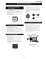
Page 98: ...e modules Please contact your local Sony Service organisation for the latest information Read restore and compare NVM contents via the I2C bus Acknowledge check of all I2C devices in the TV set Read Error Codes emulation of the Error Reader tool Remote Commander emulation User programmable Functional Check through Infrared Fast and documented Test Mode setting of all Sony TV chassis Partnumbers TR...

Reviews: