background image

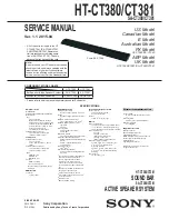
HT-CT380/CT381

5

DESTINATION  ABBREVIATIONS

The following abbreviations for model destinations are used in this 
service manual.

• Abbreviations
 AUS : 

Australian 

model

  CND  : Canadian model
  E3 

: African and Iranian models

  EA3  : Saudi Arabia, UAE, Kuwait, Iraqi, Kenyan, Tanzanian and 

Nigerian models

  SP 

: Singapore model

ADVANCE  PREPARATION  WHEN  CONFIRMING  OP-
ERATION

All of the units included in the HT-CT380/CT381 (SA-CT380/
CT381, SA-WCT380/WCT381, Remote control) are required to 
con

fi

 rming operation of SA-CT380/CT381. Check in advance that 

you have all of the units.

NOTE  OF  REPLACING  THE  KEY  BOARD

When the KEY board is defective, replace the complete mounted 
board.

NOTE  OF  REPLACING  THE  IC1009,  IC1010,  IC1012,  
IC2008,  IC2009  AND  IC3109  ON  THE  MAIN  BOARD

IC1009, IC1010, IC1012, IC2008, IC2009 and IC3109 on the 
MAIN board cannot replace with single. When these parts are 
damaged, replace the complete mounted board.

NOTE  OF  REPLACING  THE  IC3001  ON  THE  MAIN  
BOARD  AND  THE  COMPLETE  MAIN  BOARD

When IC3001 on the MAIN board and the complete MAIN board 
are replaced, it is necessary to spread the compound between the 
MAIN board and the heat sink.
Spread the compound referring to the 

fi

 gure below.

– MAIN Board (Side A) –

IC3001

compound

NOTES  ON  THE  WIRELESS  CONNECTION (LINK)  AFTER  
REPAIRS  ARE  COMPLETE

When the parts below is replaced, the wireless connection (LINK) 
of the Bar speaker and Subwoofer will be disconnected.
Before returning repaired products to the customer, follow the pro-
cedure below to LINK the Bar speaker and Subwoofer.
Also, if only the Bar speaker or Subwoofer is brought in for repair 
and the parts below are replaced, be sure to inform the customer 
when returning the repaired products that the customer must LINK 
the Bar speaker and Subwoofer.
(Indicate that the LINK procedure is described in the operating 
instructions)

Parts in which the LINK will be disconnected due to re-
placement:

•  Complete MAIN board
•  IC1002 on the MAIN board (microprocessor)
•  RF modulator (SWA12-4V TX) (Ref. No. RF1)

Linking the system (Link to the Subwoofer)

Set up the wireless subwoofer 
connection again.

1

Press MENU.

2

Select [WS] with 

j


„

 (select), then 

press ENTER.

3

Select [LINK] with 

j


„

 (select), then 

press ENTER.

4

When [START] appears on the 
display, press ENTER.

[SEARCH] appears, and the Bar 
Speaker searches for a device that 
can be used with Link. Proceed to 
the next step within 1 minute.
To quit the Link function while 
searching for a device, press BACK.

5

Press LINK on the subwoofer.

The on/standby indicator on the 
subwoofer lights up in green. [OK] 
appears on the display of the Bar 
Speaker.
If [FAILED] appears, check to ensure 
the subwoofer is turned on and 
perform the process again from 
step 1.

6

Press MENU.

The menu turns off.

IF  “PRTECT (PROTECT)”  APPEARS  ON  THE  FRONT  
PANEL  DISPLAY  OF  THE  BAR  SPEAKER

‚

Press the 

Ò

/

Æ

 (on/standby) button 

on the Bar Speaker to turn off the 
system. After the display stops 
flashing, disconnect the AC power 
cord (mains lead) then check that 
nothing is blocking the ventilation 
holes of the Bar Speaker.

Ver. 1.1

Summary of Contents for HT-CT380

Page 1: ...o Video Remote Control Profile Supported Codecs3 SBC4 AAC5 Transmission range A2DP 20Hz 20 000Hz Samplingfrequency 44 1 kHz 1 The actual range will vary depending on factors such as obstacles between devices magnetic fields around a microwave oven static electricity cordless phone reception sensitivity operating system software application etc 2 BLUETOOTH standard profiles indicate the purpose of ...
Page 2: ...MI Logoaretrademarksorregistered trademarksofHDMILicensingLLCinthe United States and other countries The N Mark is a trademark or registered trademark of NFC Forum Inc in the United States and in other countries Android and Google Play are trademarks of Google Inc Copyrights and Trademarks Apple theApplelogo iPhone iPod and iPod toucharetrademarksofAppleInc registered in the U S and other countrie...

Page 3: ...ock Diagram AMP Section 33 5 4 Block Diagram PANEL POWER SUPPLY Section 34 5 5 Printed Wiring Boards MAIN Section 1 2 36 5 6 Printed Wiring Board MAIN Section 2 2 37 5 7 Schematic Diagram MAIN Section 1 6 38 5 8 Schematic Diagram MAIN Section 2 6 39 5 9 Schematic Diagram MAIN Section 3 6 40 5 10 Schematic Diagram MAIN Section 4 6 41 5 11 Schematic Diagram MAIN Section 5 6 42 5 12 Schematic Diagram...

Page 4: ...e and perform the operation check in the volume state as low as possible CAPACITOR ELECTRICAL DISCHARGE PROCESSING When checking the board for the electric shock prevention con nect the resistors to both ends of respective capacitors to discharge the capacitor Note 1 When the connector that connects the POWER board to the MAIN board is disconnected before discharging completely finish dis charging...

Page 5: ...fore returning repaired products to the customer follow the pro cedure below to LINK the Bar speaker and Subwoofer Also if only the Bar speaker or Subwoofer is brought in for repair and the parts below are replaced be sure to inform the customer when returning the repaired products that the customer must LINK the Bar speaker and Subwoofer Indicate that the LINK procedure is described in the operat...

Page 6: ...the figure below POWER board C902 or C906 C903 or C908 C904 or C905 C907 or C988 C914 or C915 C967 C970 C976 C978 C980 C990 D901 LF901 R914 R944 TH901 VDR901 C978 C980 Except US and Canadian models only POWER Board Component Side C914 915 C902 906 C903 908 C907 988 D901 TH901 LF901 C904 905 VDR901 R914 R944 C967 C970 C990 C976 C980 C978 Except US and Canadian models only Ver 1 1 ...

Page 7: ...BLUETOOTH MODULE BT1 Page 19 2 8 KEY BOARD BLOCK Page 14 2 9 BUTTON KEY BOARD Page 15 2 11 MAIN BOARD Page 17 2 2 CABINET TOP BLOCK Page 8 2 15 SERVICE POSITION Page 21 2 3 LOUDSPEAKER 6 cm L CH R CH SP1 SP2 Page 9 2 4 NFC MODULE NFC1 Page 10 2 5 DISPLAY BOARD Page 11 2 6 POWER BOARD Page 12 2 7 CONNECTION CABLE WITH SPEAKER L CH R CH SPC1 SPC2 Page 13 2 10 RF MODULATOR RF1 Page 16 ...

Page 8: ... side protrusion Push 5 Push the protrusion and remove the terminal wide side protrusion Push 5 Push the protrusion and remove the terminal wide side 5 Push the protrusion and remove the terminal narrow side protrusion Push loudspeaker 6 cm R ch SP2 LUH VHWWLQJ red wide side black narrow side OH LEOH IODW FDEOH VHWWLQJ CN1002 flexible flat cable FFC3 filament tape sub material front side terminal ...

Page 9: ... outside inside RXGsSeDNeU FP FK 63 setting narrow terminal side wide terminal side 2 loudspeaker 6 cm L ch SP1 1 four screws 3 5 loudspeaker 6 cm L ch SP1 front side DEinet tRS ERttRP YieZ inside outside rear side cabinet top block left side right side front side Note 2 Please spread a sheet under a unit not to injure cabinet top Note 1 When installing the loudspeaker 6 cm R ch SP2 check the pres...

Page 10: ...raight into the interior flexible flat cable connector OK colored line Insert at a slant flexible flat cable connector NG How to install the flexible flat cable When installing the flexible flat cable ensure that the colored line is parallel to the connector after insertion How to install the NFC module NFC1 Note Please spread a sheet under a unit not to injure cabinet top 4 sheet NFC 2 Peel off t...

Page 11: ...inet top block left side right side front side colored line Insert straight into the interior flexible flat cable connector OK colored line Insert at a slant flexible flat cable connector NG How to install the flexible flat cable When installing the flexible flat cable ensure that the colored line is parallel to the connector after insertion lexible flat cable C settinJ 3acNinJ C settinJ DISPLAY b...

Page 12: ...talled will damage it LUH VHWWLQJ Note 3 Do not pass the wire close to the heat sink MAIN board CN1005 wiring stopper cushion CZ2 A CN3002 CN3005 heat sink heat sink 2 connector CN1005 Note 2 Before connect this connector refer to CAPACITOR ELECTRICAL DISCHARGE PROCESSING on page 4 XVKLRQ VHWWLQJ Note 4 Paste the cushion CZ2 A to screw head and wiring stopper wiring stopper screw head cushion CZ2 ...

Page 13: ...is a possibility that using this unit without the connector correctly installed will damage it 2 connector CN3002 2 connector CN3001 3 connection cable with speaker R ch SPC2 3 connection cable with speaker L ch SPC1 1 cushion CZ2 A RQQHFWLRQ FDEOH ZLWK VSHDNHU 5 FK 63 VHWWLQJ Push Push Push CN3001 Vent hole Note Do not block the vent hole in the connection cable with speaker R ch SPC2 RQQHFWLRQ F...

Page 14: ...stall the connector Insert the connector straight into the interior There is a possibility that using this unit without the connector correctly installed will damage it How to install the KEY board block cabinet bottom block bracket BTN CZ2 screw hole cabinet bottom assy five buttons button CZ2 3 Remove the KEY board block in the direction of the arrow screw hole Note Align five buttons into the h...

Page 15: ...2 A Note 2 Do not press this area during affixing Note 1 Align to cover total nine ribs as shown KEY board five tact switches four ribs five ribs Insert only part way Insert straight into the interior connector Insert at a slant connector connector connector connector connector OK NG NG RZ WR LQVWDOO WKH FRQQHFWRU Insert the connector straight into the interior There is a possibility that using th...

Page 16: ...H IODW FDEOH VHWWLQJ Terminal face is below side connector CN1003 cabinet bottom block colored line Insert straight into the interior flexible flat cable connector OK colored line Insert at a slant flexible flat cable connector NG RZ WR LQVWDOO WKH IOH LEOH IODW FDEOH When installing the flexible flat cable ensure that the colored line is parallel to the connector after insertion Note When the RF ...

Page 17: ...HE IC3001 ON THE MAIN BOARD AND THE COMPLETE MAIN BOARD on page 5 2 connector CN1005 Note 4 Before connect this connector refer to CAPACITOR ELECTRICAL DISCHARGE PROCESSING on page 4 colored line Insert straight into the interior flexible flat cable connector OK colored line Insert at a slant flexible flat cable connector NG RZ WR LQVWDOO WKH IOH LEOH IODW FDEOH When installing the flexible flat c...

Page 18: ...UG VHWWLQJ power cord AC1 cord bushing FBS001 claw 70 5 0 mm to POWER board claw Claw is on the lower side Note When installing the power cord AC1 check the direction of claw of cord bushing FBS001 and install correctly cabinet bottom block Insert only part way Insert straight into the interior connector connector Insert at a slant connector connector connector connector OK NG NG RZ WR LQVWDOO WKH...

Page 19: ...the QoQ woveQ IaEriF 7 le iEle Ilat FaEle VettiQJ bluetooth module BT1 flexible flat cable 14 core FFC1 Terminal face is below side colored line Insert straight into the interior flexible flat cable connector OK colored line Insert at a slant flexible flat cable connector NG ow to iQVtall the Ile iEle Ilat FaEle When installing the flexible flat cable ensure that the colored line is parallel to th...

Page 20: ... IODW FDEOH VHWWLQJ Terminal face is below side connector CN2001 4 Remove the chassis MAIN block in the direction of the arrow colored line Insert straight into the interior flexible flat cable connector OK colored line Insert at a slant flexible flat cable connector NG RZ WR LQVWDOO WKH IOH LEOH IODW FDEOH When installing the flexible flat cable ensure that the colored line is parallel to the con...

Page 21: ...HT CT380 CT381 21 2 15 SERVICE POSITION MAIN board POWER board ...

Page 22: ... 2 1 Panel Test Mode It can check the lighting of fluorescent indicator tube and LED operation of buttons display of model name destination and soft ware version Procedure 1 Enter the test mode menu Refer to Setting method of the test mode menu 2 In the state of blinking the PANEL on the fluorescent indica tor tube press the INPUT button 3 All segments in the fluorescent indicator tube and LED Blu...

Page 23: ...els CE2 7 When INPUT button is pressed while the each version is dis played on the fluorescent indicator tube year month and day of the software creation is displayed on the fluorescent indica tor tube Displayed values in the above figure are example When INPUT button is pressed again the display returns to the each version display Releasing method Press the 1 button to release the test mode menu ...

Page 24: ...MP Test Mode It is displayed AMP on the fluorescent indicator tube Not used for the servicing Press the 1 button if having entered this mode 2 9 Tone Test Mode It can check the test tone output from each speaker Preparation Connect the Bar Speaker SA CT380 CT381 and the Subwoofer SA WCT380 381 by wireless Procedure 1 Enter the test mode menu Refer to Setting method of the test mode menu on page 22...

Page 25: ...t the WS TST press the INPUT button 3 The message FACTRY is displayed on the fluorescent indi cator tube and enter the wireless sound test mode 4 Press the V v buttons on the remote commander select the VER CHE and press the ENTER button on the remote commander 5 The com version of Subwoofer SA WCT380 WCT381 is displayed on the fluorescent indicator tube Displayed values in the above figure are ex...

Page 26: ...ormation Procedure 1 Enter the test mode menu Refer to Setting method of the test mode menu on page 22 2 Press the VOLUME VOLUME buttons to select the RESET press the INPUT button 3 The message RESET is displayed on the fluorescent indica tor tube then turn the power off ...

Page 27: ... voltage of the following is 12 V MAIN board IC3003 pin 4 No Yes Replace the IC1002 on the MAIN board Yes No No No No OUT_D line pin 27 28 OUT_C line pin 32 OUT_B line pin 35 and OUT_A line pin 39 40 of IC3001 on the MAIN board do not short circuits or opens Replace the IC3001 on the MAIN board Yes Replace the IC3001 on the MAIN board Yes Yes Mounted parts on the OUT_D line pin 27 28 OUT_C line pi...

Page 28: ...MAIN board 3 Power is not turned on Power is not turned on The voltage of the following is 28 V POWER board CN902 pin 3 to 5 The voltage of the following is 12 to 17 V POWER board CN902 pin 9 The voltage of the following is 3 3 V MAIN board IC1002 pin 96 97 Yes POWER board is damaged Yes Yes Vibrator X1001 on the MAIN board is oscillated after AC input Yes Fuse F901 F931 on the POWER board conduct...

Page 29: ...AIN board No Check the mounted state of coil L3109 to L3114 on the MAIN board Check the IC3109 on the MAIN board and replace the complete MAIN board The voltage of the following is 3 3 V MAIN board CN3100 CN3101 CN3102 CN3106 pin 13 CEC Check the diode D1010 and IC1002 on the MAIN board Yes Yes No The voltage of the following TMDS input line is about 3 0 V MAIN board IC3109 pin 24 to 31 In the cas...

Page 30: ...HT CT380 CT381 30 MEMO ...

Page 31: ...T PLUG DET 18 5V POWER 13 CEC 27 R2X0 26 R2X0 29 R2X1 28 R2X1 31 R2X2 30 R2X2 25 R2XC 24 R2XC 59 DSDA2 60 DSCL2 61 CBUS_HPD2 62 R2PWR5V 7 DATA0 9 DATA0 4 DATA1 6 DATA1 1 DATA2 3 DATA2 10 CLOCK 12 CLOCK 16 SDA 5V 15 SCL 5V 19 HOT PLUG DET 18 5V POWER 13 CEC CN3100 3 CN3102 2 CN3101 1 19 R1X0 45 HDMI_SDA 53 CSCL 46 HDMI_SCL 45 INT 56 HDMI_INT 43 RESET_N 50 RSVDH 54 HDMI_RST 15 CEC_I O 18 R1X0 21 R1X...

Page 32: ...MUTE 73 BT_RST 42 RTS1 MC_BT_CTS0 32 BT_UART_TX L_OUT L_OUT R_OUT BT_UART_RX BT_UART_RTS BT_UART_CTS MUTE RESET BT1 Bluetooth MODULE R_OUT SL SR_IN 40 MPIO_B1 12 C SW_IN 58 MPIO_B2 13 SBL SBR_IN 62 MPIO_B3 14 DIR_IN 65 ANALOG AUDIO SELECTOR IC2003 A X0 12 X1 14 Y1 5 Y0 1 X 13 Y 3 10 C SW1_OUT 56 BCLK_OUT 60 LRCLK_OUT 61 XTAL 13 CLKIN 12 SCKO 20 BCK 19 LRCK 18 NPCM 2 DIR_ERROR 25 HDMI_MUTE_ON 55 HD...

Page 33: ...K DSP_BCK AMP_D1FLFR AMP_D3CSW MCK DSP_BCK DSP_LRCK 002B BUFFER Q3002 PWM_M_2 40 DIGITAL POWER AMP IC3001 INPUT_D OUT_D 15 INPUT_C 14 INPUT_B 6 INPUT_A 5 27 OUT_D 28 OUT_C 32 OUT_B 35 PW_VACS_DET 63 OUT_A 39 PWM_P_2 41 VALID 37 PWM_M_4 48 PWM_P_4 49 DC DETECT Q3003 THERMAL DETECT Q950 952 DC DETECT Q3001 SP2 R CH SP1 L CH L3001 L3004 L3003 L3002 OUT_A 40 TH902 Except US CND MUTE PDN RESET DRIVE_OC...

Page 34: ... CONVERTER IC2012 DC DC CONVERTER IC3705 VDD 59 P_CONT3 DD12V 12V REGULATOR IC1011 E12V VOLTAGE DETECT IC1003 RESET SWITCH Q1002 BT3 3V 43 PCONT_BT 3 3V REGULATOR IC2007 MFI3 3V 3 3V REGULATOR IC1013 23 HDMI_TX_5VPWR HDMI_TX_5V DD6V HDMI5V 5V REGULATOR IC3107 5V REGULATOR IC3102 DIR5V SW3 3V 3 3V REGULATOR IC1008 SW4V B SWITCH Q1007 1008 3 3V REGULATOR IC803 DC DC CONVERTER D803 805 Q802 78 P_CONT...

Page 35: ...waveforms Signal path F AUDIO ANALOG J AUDIO DIGITAL E VIDEO N Bluetooth For Printed Wiring Boards Note X Parts extracted from the component side Y Parts extracted from the conductor side f Internal component Pattern from the side which enables seeing The other layers patterns are not indicated Caution Pattern face side SIDE B Parts face side SIDE A Parts on the pattern face side seen from the pat...

Page 36: ... R1035 R1038 C2004 C2005 Q2002 C2006 Q2003 R1040 C2009 CL3001 CL3002 CL3003 R1047 CL3004 R1048 C2010 CL3005 R1049 C2011 CL3006 C2012 CL3007 C2013 CL3008 C2015 C2018 C2019 R3187 R1053 R3188 R1054 R3189 R1055 C2020 C2021 C2022 C2023 R3190 R3191 C2025 R3192 C2026 D2003 C2027 R1060 C2028 R3195 R1061 D2005 C2029 R1062 R1063 R3198 R1064 R3199 R1065 R2007 R2009 C2032 C2033 IC2004 C2034 C2035 IC2006 C2036...

Page 37: ... JL2014 C3175 IC1011 JL1075 R3729 JL2015 C3176 JL1076 JL2016 C3177 IC1013 JL1077 JL2017 JL1078 JL2018 JL1079 JL2019 R1020 R3155 R1022 C3180 JL1080 JL2020 C3181 JL1081 JL2021 JL1082 R1026 JL2022 JL1083 JL2023 C3184 JL1084 R1028 JL2024 C3185 JL2025 JL2026 JL2027 C1054 JL2028 C1055 JL2029 R3162 R1030 C1059 R1031 R1032 JL2030 JL2031 JL2032 R1037 JL2033 C1060 JL2034 C1061 JL2035 C2002 JL2036 C2003 JL20...

Page 38: ...6 1k 2 2k R3235 130k R3236 R3194 10k 0 R3248 0 R3250 10k R3137 47 R3260 47 R3261 47 R3262 47 R3263 47 R3264 0 R3176 100 R3204 10k R3273 10k R3274 10k R3275 3 3k R3215 15k R3189 100 R3203 100 R3216 47 R3284 330 R3285 47 R3214 100 R3287 100 R3288 0 R3182 0 R3162 4 7k R3291 10k R3187 R3206 1 8k 0 R3293 10k R3294 10k R3295 10k R3296 10k R3297 47 R3300 330 R3301 100 R3188 10k R3192 10k R3302 R3198 0 1k...

Page 39: ...H L2004 10uH L2002 LTC014EUBFS8TL Q2001 220 R2021 47k R2034 1k R2064 47k R2033 100 R2059 100 R2058 100 R2057 0 R2009 10k R2004 100k R2011 100 R2054 100 R2050 100 R2048 10k R2005 100k R2010 100 R2019 R2013 47k 100k R2046 R2042 1k 4 7k R2052 47k R2016 R2044 47k 47k R2017 100 R2018 100k R2045 R2055 100 100 R2032 100 R2022 100 R2023 100 R2025 220 R2020 100 R2049 100 R2051 56k R2134 3 3k R2038 4 7k R20...

Page 40: ... VDD_INT 76 VDD_INT 77 FLAG0 78 VDD_INT 79 VDD_INT 80 FLAG1 81 FLAG2 82 FLAG3 83 MLBCLK 84 MLBDAT 85 MLBDO 86 VDD_EXT 87 MLBSIG 88 VDD_INT 89 MLBSO 90 TRST 91 EMU 92 TDO 93 VDD_EXT 94 VDD_INT 95 TDI 96 TCK 97 VDD_INT 98 RESET 99 TMS 100 VDD_INT JL2031 JL2024 JL2039 JL2038 JL2037 JL2032 JL2034 JL2028 JL2022 JL2033 JL2023 JL2035 JL2030 JL2036 JL2027 JL2040 JL2025 JL2029 JL2026 10uH L2007 L2008 0 68u...

Page 41: ...VSS1_CORE 36 VALID 37 PWM_M_1 38 PWM_P_1 39 PWM_M_2 40 PWM_P_2 41 PWM_M_3 42 PWM_P_3 43 NC_44 44 NC_45 45 NC_46 46 NC_47 47 PWM_M_4 48 PWM_P_4 49 AVDD_PWM 50 AVSS_PWM 51 VR_PWM 52 NC_53 53 NC_54 54 NC_55 55 NC_56 56 100 R3040 100 R3033 100 R3031 100 R3041 100 R3032 100 R3042 100 R3030 100 R3029 0 01 C3044 0 0047 C3048 100 R3035 100 R3037 100 R3036 100 R3038 100 R3039 10 C3035 1 C3001 1 C3047 16V 1...

Page 42: ...R1027 R1062 100 R1050 10k 100 R1029 R1021 100 R1014 1k 100 R1025 10k R1001 100 R1059 100 R1159 100 R1157 0 R1033 47k R1037 R1005 47k 10k R1031 R1107 4 7k R1018 100k 10k R1042 10k R1002 2 2k R1164 2 2k R1163 3 3k R1161 100 R1060 SD RX_MUTE DC_PRT HDMI_5VPWR HDMI_RST OVF1 BT_RTS PCONT_HDMI DIR_ZERO DIR_DO DIR_XSTATE DIR_ER HDMI_INT HDMI_SCL DSP_TXD DSP_INT SPI_MISO SF_HOLD PCONT_BT DSP_RXD DIR_RST H...

Page 43: ...J 4 CE 5 RT8295ALZSP IC1009 BOOT 1 VIN 2 SW 3 GND 4 FB 5 COMP 6 EN 7 SS 8 MFI337S3959 IC1010 GND 1 SDA 2 NC_3 3 NC_4 4 NC_5 5 SCL 6 RST 7 VCC 8 R1167 0 4P CN1009 1 DGND 2 KEY0 3 KEY1 4 KEY2 18P CN1002 DGND 1 SIRCS2 2 E4V 3 SIRCS 4 DGND 5 FL_CLK 6 FL_CS 7 FL_DATA 8 DD12V 9 SW6V 10 FL_GND 11 FL_GND 12 RST_FL 13 NFC_SCL 14 DGND 15 NFC_SDA 16 NFC_IRQ 17 NFC_RFDET 18 JL1021 100 R1101 JL1019 100 R1106 J...

Page 44: ...0 C821 C822 C823 C824 C825 D802 D803 D804 D805 D806 D807 3 1 IC801 IC803 Q802 L801 ND801 FLUORESCENT INDICATOR TUBE JL801 JL805 JL808 JL809 JL810 JL811 JL812 JL813 JL814 JL815 JL816 JL817 JL818 JL819 JL820 JL821 JL822 JL823 JL824 JL825 JL826 JL827 JL828 JL829 JL830 JL831 JL832 JL833 JL834 JL835 JL836 DISPLAY BOARD COMPONENT SIDE DISPLAY BOARD CONDUCTOR SIDE 1 894 320 11 11 1 894 320 11 11 K A K A ...

Page 45: ... NFC_RFDET 2 NFC_IRQ 3 NFC_SDA 4 DGND 5 NFC_SCL 6 RST_FL 7 FL_GND 8 FL_GND 9 SW6V 10 DD12V 11 FL_DATA 12 FL_CS 13 FL_CLK 14 DGND 15 SIRCS 16 E4V 17 SIRCS2 18 DGND 10 C801 47 R802 47 R803 47 R804 47 R801 100 R805 100 R808 100 R806 100 R807 DA2J10100L D802 47 R812 22k R813 47 R811 10 C810 1 C813 10k R814 10k R817 0 R815 RB520SM 30T2R D804 1 C816 1 C821 1 C819 1 C817 1 C811 1 C812 1 C815 1 C814 33k R...

Page 46: ...6 C937 R976 R977 R978 R987 JL936 JL937 R997 C965 C968 C971 JL973 JL974 D930 JL975 D931 JL976 D932 JL977 JL978 D934 JL979 D935 D936 D937 D939 3 1 2 4 C904 C905 C907 C988 C903 C908 C902 C906 C935 C938 C914 C915 POWER BOARD 1 894 322 11 11 LND001 PATTERN SPARK GAP CHASSIS E A A A A A E K K K A A K A K K K A A K K A US CND C E A K K K K A E E Except US CND Except US CND CHASSIS MAIN BOARD CN1005 02P U...

Page 47: ...64M 400 D937 RR264M 400 D936 0 1 C936 1k R965 1k R987 1 5k R976 47k R977 220k R971 4 7k R978 0 01 C971 35V C980 47 R951 220k R952 1k 50V C978 10 Q952 2PA1576R 115 Q950 35V C976 47 35V 2200 C967 250V C965 0 0047 E ET932 R934 R932 R944 0 1 C930 2SC5053T100Q Q930 LTC044EUBFS8TL Q931 KDZTR18B D972 UDZSUSTE 1730B D935 DZ2J180M0L D934 DZ2J24000L D939 UDZSUSTE 1730B D931 DZ2J180M0L D930 FMX 22SL D965 25V...

Page 48: ... 36 MPIO_C3 10 VINR 48 VINL 47 VCOM 44 RST 34 RXIN2 33 RXIN3 32 RXIN6 ALRCKIO 29 RXIN7 ADIN0 28 RXIN2 AGNDAD 45 VCCAD 46 VCC 42 FILT 43 AGND 41 MPIO_C2 9 MPIO_C1 8 MPIO_C0 7 RXIN0 37 RXIN3 RXIN4 RXIN5 RXIN6 RXIN7 AUXIN0 RXIN8 MPIO_A MPIO_B MPIO_C MPO0 MPO1 RXIN8 RXIN9 RXIN10 RXIN11 DTOUT RXIN0 A D CONVERTER A D CONVERTER MODE CONTROL DIR ANALOG XMCKO DIVIDER CLOCK DATA RECOVERY LOCK DETECTION MPO0...

Page 49: ...PWM TIMING CONTROL PWM RECEIVER PWM RECEIVER PWM RECEIVER PWM RECEIVER PWM TIMING CONTROL GATE DRIVE CLIP 18 FAULT 16 M3 21 M2 20 M1 19 GVDD_CD 22 BST_X GVDD_X AVDD DVDD I2C SERIAL CONTROL INTERFACE CLOCK PLL AND SERIAL DATA INTERFACE PWM_HPM_L 1 PWM_HPP_L 2 PWM_HPM_R 3 PWM_HPP_R 4 PLL_FLTM 6 PLL_FLTP 7 LRCLK 22 SCLK 23 SDIN1 24 SDIN2 25 SDIN3 26 SDIN4 27 VR_DIG 28 RESET 16 HP_SEL 17 PDN 18 MUTE A...

Page 50: ...6735 US and Canadian models IC930 STR Y6766B Except US and Canadian models DISPLAY Board IC803 MM3411A33URE VOUT 3 CE 1 GND 2 VDD 4 VOLTAGE REFERENCE CURRENT LIMIT BIAS D ST 1 S OCP 2 VCC 3 GND 4 BD 6 FB OLP 5 STARTUP LOGIC DRIVER LATCH OVERCURRENT PROTECTION BOTTOM SKIP UNDER VOLTAGE LOCK OUT REGULATOR CONSTANT CURRENT FEEDBACK STANDBY OVERLOAD PROTECTION BOTTOM DETECTION NF 7 OSCILLAOTR Ver 1 1 ...

Page 51: ...mplifier H power on 27 DAMP_SCL O Serial data transfer clock signal output to the stream processor 28 DAMP_SDA I O Two way data bus with the stream processor 29 M_TX_OUT O Serial data output to the DSP 30 M_RX_IN I Serial data input from the DSP 31 SCD CLK1 I Serial data transfer clock signal input terminal for flash memory writing 32 RTS1 MC_BT_CTS0 I Clear to send signal input from the Bluetooth...

Page 52: ...O Serial data output to the fluorescent indicator tube 76 FL_CS O Chip select signal output to the fluorescent indicator tube 77 FL_CLK O Serial data transfer clock signal output to the fluorescent indicator tube 78 P_CONT_HDMI O Power on off control signal output terminal for the HDMI section H power on 79 CP_RESET O Reset signal output to the MFI L reset 80 P_CON_DSP O Power on off control signa...

Page 53: ...ot used 29 VDD_INT Power supply terminal 1 1V for core 30 UART_OUT O Serial data output to the system controller 31 UART_IN I Serial data input from the system controller 32 LED Not used 33 34 DPI_P12 DPI_P13 Not used 35 DAI_P03 Not used 36 DPI_P14 Not used 37 to 39 VDD_INT Power supply terminal 1 1V for core 40 SL SR_IN I Audio signal for surround L ch R ch input from the digital audio interface ...

Page 54: ... controller 78 79 VDD_INT Power supply terminal 1 1V for core 80 FLAG1 I Error detection signal input terminal L error 81 FLAG2 I Audio setting signal input terminal L LPCM audio H HBR audio 82 FLAG3 Not used 83 MLBCLK Not used 84 MLBDAT Not used 85 MLBDO Not used 86 VDD_EXT Power supply terminal 3 3V for I O 87 MLBSIG Not used 88 VDD_INT Power supply terminal 1 1V for core 89 MLBSO Not used 90 TR...

Page 55: ...IN 1 connector 29 R2X1 I TMDS data positive input from the HDMI IN 1 connector 30 R2X2 I TMDS data negative input from the HDMI IN 1 connector 31 R2X2 I TMDS data positive input from the HDMI IN 1 connector 32 CVDD10 Power supply terminal 1V 33 AVDD10 Power supply terminal 1V 34 AVDD33 Power supply terminal 3 3V 35 R3XC I TMDS clock negative signal input from the HDMI IN 2 connector 36 R3XC I TMDS...

Page 56: ... clock positive signal output to the ARC HDMI OUT connector 79 TX0 O TMDS data negative output to the ARC HDMI OUT connector 80 TX0 O TMDS data positive output to the ARC HDMI OUT connector 81 TDVDD10 Power supply terminal 1V 82 TX1 O TMDS data negative output to the ARC HDMI OUT connector 83 TX1 O TMDS data positive output to the ARC HDMI OUT connector 84 TX2 O TMDS data negative output to the AR...

Page 57: ...n of Appearance Parts Ex ample KNOB BALANCE WHITE RED Parts Color Cabinet s Color 6 1 OVERALL SECTION Bottom view The components identified by mark 0 or dotted line with mark 0 are critical for safety Replace only with part number specified Les composants identifiés par une marque 0 sont critiques pour la sécurité Ne les remplacer que par une pièce por tant le numéro spécifié The components identi...

Page 58: ...NEL SIDE LS ASSY Left side CT381 FFC3 1 970 611 11 WIRE KIT BAR FFC 18P See Note FFC4 1 970 611 11 WIRE KIT BAR FFC 6P See Note NFC1 8 989 602 00 RC S730 WW NFC module SP1 1 859 120 11 LOUDSPEAKER 6 cm L ch SP2 1 859 120 11 LOUDSPEAKER 6 cm R ch 2 7 685 646 79 SCREW BVTP 3X8 TYPE2 IT 3 Ref No Part No Description Remark Ref No Part No Description Remark Note As for WIRE KIT BAR FFC all flat flexibl...

Page 59: ...R FFC 24P See Note 2 RF1 1 492 347 11 RF MODULATOR SWA12 4V TX See Note 3 SPC1 1 848 866 11 CONNECTION CABLE WITH SPEAKER L ch SPC2 1 848 866 21 CONNECTION CABLE WITH SPEAKER R ch 1 7 685 647 79 SCREW BVTP 3X10 TYPE2 IT 3 3 7 685 146 11 SCREW P 3X8 TYPE2 NON SLIT Ref No Part No Description Remark Ref No Part No Description Remark Note 2 As for WIRE KIT BAR FFC all flat flexible cables Ref No FFC1 ...

Page 60: ...8 TYPE2 IT 3 4 7 682 546 09 SCREW B 3X5 Ref No Part No Description Remark Ref No Part No Description Remark Note 1 When the complete MAIN board is replaced refer to NOTE OF REPLACING THE IC3001 ON THE MAIN BOARD AND THE COMPLETE MAIN BOARD and NOTES ON THE WIRELESS CONNECTION LINK AFTER REPAIRS ARE COMPLETE on page 5 Note 2 When the complete POWER board is replaced refer to BOND FIXATION OF ELECTR...

Page 61: ...5 1 216 864 11 SHORT CHIP 0 R816 1 216 839 11 METAL CHIP 33K 5 1 10W R817 1 216 833 11 METAL CHIP 10K 5 1 10W R818 1 216 797 11 METAL CHIP 10 5 1 10W R819 1 216 797 11 METAL CHIP 10 5 1 10W R820 1 250 535 11 METAL CHIP 47K 1 1 16W A 2063 684 A KEY BOARD COMPLETE When the KEY board is defective replace the complete mounted board 9 A 2076 756 A MAIN BOARD COMPLETE SV CT381 See Note 9 A 2076 757 A MA...

Page 62: ... C2020 1 118 387 11 CERAMIC CHIP 0 068uF 10 16V C2021 1 118 386 11 CERAMIC CHIP 0 1uF 10 16V C2022 1 118 386 11 CERAMIC CHIP 0 1uF 10 16V C2023 1 116 720 11 CERAMIC CHIP 10uF 20 6 3V C2024 1 116 720 11 CERAMIC CHIP 10uF 20 6 3V C2025 1 164 874 11 CERAMIC CHIP 100PF 5 50V C2026 1 164 874 11 CERAMIC CHIP 100PF 5 50V C2027 1 164 858 11 CERAMIC CHIP 22PF 5 50V C2028 1 165 492 21 ELECT CHIP 100uF 20 10...

Page 63: ...108 1 118 035 11 CERAMIC CHIP 0 1uF 10 25V C3114 1 118 035 11 CERAMIC CHIP 0 1uF 10 25V C3115 1 116 737 11 CERAMIC CHIP 1uF 20 10V C3121 1 116 737 11 CERAMIC CHIP 1uF 20 10V C3127 1 118 035 11 CERAMIC CHIP 0 1uF 10 25V C3128 1 116 720 11 CERAMIC CHIP 10uF 20 6 3V C3129 1 116 720 11 CERAMIC CHIP 10uF 20 6 3V C3130 1 118 035 11 CERAMIC CHIP 0 1uF 10 25V C3133 1 116 720 11 CERAMIC CHIP 10uF 20 6 3V C...

Page 64: ...EMOVAL SMD IC IC1001 6 721 894 01 IC BR24G16FJ 3GTE2 IC1002 A 2076 761 A IC R5F3650RDFB 30 SV See Note 1 IC1003 6 713 333 01 IC PST8429UL IC1008 6 717 680 01 IC BD00IC0WEFJ E2 IC1009 Not supplied IC RT8295ALZSP See Note 2 IC1010 Not supplied IC MFI337S3959 See Note 2 IC1011 6 712 825 01 IC R1154N001C TR FE IC1012 Not supplied IC BMA250E Except US CND See Note 2 IC1013 6 719 198 01 IC MM3411A33URE ...

Page 65: ...27 1 218 941 81 METAL CHIP 100 5 1 16W R1028 1 218 977 11 METAL CHIP 100K 5 1 16W R1029 1 218 941 81 METAL CHIP 100 5 1 16W R1030 1 218 965 11 METAL CHIP 10K 5 1 16W R1031 1 218 965 11 METAL CHIP 10K 5 1 16W R1032 1 218 977 11 METAL CHIP 100K 5 1 16W R1033 1 216 864 11 SHORT CHIP 0 R1034 1 218 989 11 METAL CHIP 1M 5 1 16W R1035 1 218 977 11 METAL CHIP 100K 5 1 16W R1037 1 218 973 11 METAL CHIP 47K...

Page 66: ... 100K 5 1 16W R2013 1 218 973 11 METAL CHIP 47K 5 1 16W R2014 1 218 973 11 METAL CHIP 47K 5 1 16W R2016 1 218 973 11 METAL CHIP 47K 5 1 16W R2017 1 218 973 11 METAL CHIP 47K 5 1 16W R2018 1 218 941 81 METAL CHIP 100 5 1 16W R2019 1 218 941 81 METAL CHIP 100 5 1 16W R2020 1 218 945 11 METAL CHIP 220 5 1 16W R2021 1 218 945 11 METAL CHIP 220 5 1 16W R2022 1 218 941 81 METAL CHIP 100 5 1 16W R2023 1 ...

Page 67: ...18 941 81 METAL CHIP 100 5 1 16W R2142 1 216 864 11 SHORT CHIP 0 R2144 1 218 977 11 METAL CHIP 100K 5 1 16W R2145 1 218 941 81 METAL CHIP 100 5 1 16W R2147 1 216 864 11 SHORT CHIP 0 R2152 1 216 864 11 SHORT CHIP 0 R2155 1 216 864 11 SHORT CHIP 0 R2163 1 250 525 11 METAL CHIP 18K 1 1 16W R3001 1 250 530 11 METAL CHIP 30K 1 1 16W R3002 1 218 937 11 METAL CHIP 47 5 1 16W R3003 1 218 937 11 METAL CHIP...

Page 68: ... R3287 1 218 941 81 METAL CHIP 100 5 1 16W R3288 1 218 941 81 METAL CHIP 100 5 1 16W R3291 1 218 961 11 METAL CHIP 4 7K 5 1 16W R3293 1 216 864 11 SHORT CHIP 0 R3294 1 218 965 11 METAL CHIP 10K 5 1 16W R3295 1 218 965 11 METAL CHIP 10K 5 1 16W R3296 1 218 965 11 METAL CHIP 10K 5 1 16W R3297 1 218 965 11 METAL CHIP 10K 5 1 16W R3300 1 218 937 11 METAL CHIP 47 5 1 16W R3301 1 218 947 11 METAL CHIP 3...

Page 69: ... CND 0 IC930 6 721 976 01 IC STR Y6766B Except US CND IC931 6 716 865 01 IC MM1431FNRE COIL L966 1 460 612 11 COIL CHOKE 2 2uH L967 1 481 175 21 INDUCTOR 4 7uH LINE FILTER 0 LF901 1 445 944 11 TRANSFORMER LINE FILTER Except US CND See Note 0 LF901 1 460 693 11 LINE FILTER TRANSFORMER US CND See Note PHOTO COUPLER 0 PH930 6 600 883 01 PHOTO COUPLER EL816S1 B TA DTE S TRANSISTOR 0 Q930 8 729 056 46 ...

Page 70: ...he POWER board are replaced refer to BOND FIXATION OF ELECTRIC PARTS on page 6 Note 3 As for WIRE KIT BAR FFC all flat flexible cables Ref No FFC1 FFC2 FFC3 FFC4 will be 1 set 501 Remote control 1 502 Optical digital cable 1 503 Wall mounting brackets 2 504 Screws 2 505 Speaker pads for the subwoofer for horizontally 4 ACCESSORIES 4 565 123 12 MANUAL INSTRUCTION ENGLISH SPANISH FRENCH US CND 4 565...

Page 71: ...MEMO HT CT380 CT381 71 ...

Page 72: ...tact point of signal lines or the like in DIAGRAMS SECTION If a contact point of a BLOCK DIAGRAM PRINTED WIRING BOARD or SCHEMATIC DIAGRAM is shown in a different page use the PDF file search function to find one e g If a contact point is shown as follow the procedure below Procedure 1 Press the F key while pressing the Ctrl key 2 Input 001Z in the search box and press the Enter key 3 The relevant...

Reviews: