background image

20

4/25/00

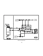
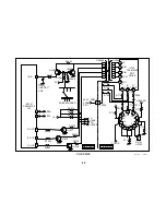
SWITCHING POWER SUPPLY

1CTV27

AC HI
FROM
RY602

C645

C646

D605

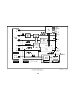
C644

C647

AC LO
FROM
T602/3

C612

R627

R628

TO
IN-RUSH CURRENT
LIMIT/PROTECT

R621

*

R626

R637 R662 R660

C617

D610

R632

R641

R633

C619

D611

R643

C652

R646

D614

D613

R638

CREATES
AUDIO B+

CREATES
LOW B+

T603

CREATES
+135

FROM
+135
ERROR
FROM
IC602/2

PH601

PC123FY2

4

3

1

2

R645

R644

IC601

STR F6624/6654

CONVERTER

D GND

VIN OCP/FB

3

5

2

4

1

S

7

8

2

3

5

4

16

17

14

13

11

12

A BOARD

C620

*ONLY FOUND IN 24" AND ABOVE MODELS.  SEE IN RUSH CURRENT PROTECTION

IN RUSH
CURRENT
PROTECT
FROM
Q602

*Q603

123.7 VDC

122.8 VDC

Summary of Contents for FD TRINITRON WEGA KV-13FM12

Page 1: ...l Circuit Description and Troubleshooting Course CTV 27 Direct View Television BA 5 Chassis Models KV 13FM12 KV 27FS12 KV 13FM13 KV 27FS16 KV 13FM14 KV 27FV16 KV 20FV12 KV 32FS12 KV 20FS12 KV 32FS16 KV 24FV12 KV 20FS12 ...

Page 2: ...Sony Service Company A Division of Sony Electronics Inc 1999 All Rights Reserved Printed in U S A S isatrademarkofSonyElectronics ...

Page 3: ...0FV12 KV 32FS12 KV 20FS12 KV 32FS16 KV 24FV12 Prepared by National Training Department Sony Service Company A Division of Sony Electronics Inc Course presented by _____________________________________ Date___________________________________________________ Student Name ___________________________________________ ...

Page 4: ... 11 Power ON 11 Degaussing 11 Shutdown 11 Table of Contents Inrush Current Protection 13 Switching Power Supply 15 Startup 15 Regulation 15 IC601 Internal Protection 17 Operating the Supply without a Load 19 Troubleshooting 21 135 OCP and H Protect 23 Latch and Hold Down 23 H Protect 23 135 Volt OCP 23 Deflection Block 25 Horizontal 25 Pincushion 25 Vertical 25 Dynamic Focus and Quadra pole 25 Hor...

Page 5: ...lter 37 Y C Processing 37 PIP 37 Audio without K Board 39 Audio Amp 39 Volume Control and Muting 39 Audio with K Board 41 Audio Iinputs and Processing 41 Audio Amp 41 Appendix Excerpt from CTV 26 Standby Power Supply i Converter Operation i Regulation i Over Current Protection OCP iii Over Voltage Protection OVP iii Secondary Output iii Checking Q621 iii ...

Page 6: ...SAP except for the 13 inch models The 13 inch models are mono and contain only one speaker All 24 and under manuals contain a headphone jack All V models contain the Steady Sound Auto Volume BBE en hancement and Dynamic Acoustic Chamber DAC features The following table shows the type of surround sound and audio output power Surround Power Output KV 13FM12 N A 3W KV 20FS12 N A 3W x 2 KV 20FV12 Matr...

Page 7: ...ment Shifts the phase of the audio signal to im prove TV sound Dynamic Acoustic Chamber DAC A speaker enclosure that uses the cabinet to improve sound quality SRS 3D A digital signal processing algorithm that simulates surround sound using only two speakers Dynamic Focus Automatically adjusts the focus to improve focus on certain parts of the screen Magnetic Quadra pole Controls the electron beam ...

Page 8: ...nd SRS Processor CA CRT Drive and N S Amp MA Syscon Y C Jungle Comb Filter Sub tuner D Dynamic Focus and Quadrapole Focus HA Front A V Inputs and Menu Switches HB IR detector HX All Switches except KV27FV16 B Board 3D Comb Filter P Board PIP Processing VA Velocity Modulation and Quadrapole Found in KV27FV16 only The differences in layout between the 24 and below and the 27 and above models are the...

Page 9: ...4 CB Board VB board A board K board KV 20FV12 KV 24FV12 only MB board CA board VA board A board K board P board B board D board 27 Inch and Over KV 27FV16 pictured 24 Inch and Under ...

Page 10: ... under sets will have a video input select switch on the A board In other models the video switching will be handled by the YCJ on the MA board Deflection The horizontal vertical and pincushion correction circuits are contained on the A board These circuits control the current through the yokes in order to correctly scan the CRT The FBT produces supply voltages for the vertical output and creates ...

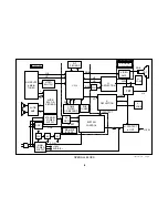
Page 11: ... J STANDBY POWER SUPPLY DGC 5V REG 12V SYSTEM CONTROL MAIN POWER SUPPLY PIN H DEFLECTION VIDEO AMP V YOKE V DEFLECTION H YOKE PIP P BOARD YUV Y C CV L R L R P ON E W RGB RGB HP HD DGC 7 5V 200V 135V HV A BOARD OVERALL BLOCK 14CTV27 1231 CRT 12V 15V 135V 5V 9V AUDIO B RESET I PROTECT VD CV Y C FBT MA or MB BOARD CA OR CB BOARD ...

Page 12: ...following fail ures occur Standby 7 5 volt OVP If over voltage occurs on this line a LOW will be output to the base of the relay drive transistor This shuts the set OFF 135 volt OCP This sensor monitors the voltage across a resistor that feeds the H Out and FBT and protects against 135 volt OCP When OCP is detected the protect latch is activated When the latch is acti vated drive to the relay is s...

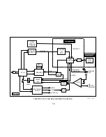
Page 13: ...C IN POWER ON STANDBY 5v REG RY602 STANDBY 7 5 SWITCHING SUPPLY AUDIO 135V LV SUPPLY OVP RELAY LATCH DGC DGC IC502 VERTICAL OUTPUT YCJ IC1702 RGB DRIVE I2 C IC1001 SYSCON HLDWN IK OCP HV DETECT FROM FBT 135 A BOARD MA MB BOARD STANDBY TIMER LED STANDBY 5V I PROTECT CA CB BOARD IC501 ...

Page 14: ...ats 1 No video 2 Sound OK White balance failure weak picture tube or Low G2 voltage Continues to blink once a second No or defective Y C Jungle IC301 communications No reply from Y C Jungle IC data bus is busy grounded or held HIGH or IK video path is defective at turn ON The set will usually act differently from what is shown in the table when it is powered up with a defect present However indica...

Page 15: ...C IN POWER ON STANDBY 5v REG RY602 STANDBY 7 5 SWITCHING SUPPLY AUDIO 135V LV SUPPLY OVP RELAY LATCH DGC DGC IC502 VERTICAL OUTPUT YCJ IC1702 RGB DRIVE I2 C IC1001 SYSCON HLDWN IK OCP HV DETECT FROM FBT 135 A BOARD MA MB BOARD STANDBY TIMER LED STANDBY 5V I PROTECT CA CB BOARD IC501 ...

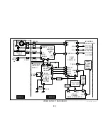
Page 16: ...ork provides the delay necessary for Reset to occur After Reset occurs IC1001 Control Tuning System begins execut ing instructions One of its first tasks is to read and load the contents of the external NVM into the registers of IC1001 via the I C bus The data in the NVM contains the service data as well as any data relating to cus tomer control settings such as volume level Power ON When the Powe...

Page 17: ...5 5V REG BA3993 5 IC1001 CONTROL TUNING SYSTEM M37273MF 258 STANDBY 7 5V CN1004 DGC RELAY VCC RY601 Q609 R634 D601 R630 R642 R663 R661 R653 C602 C601 D602 RY602 R607 Q607 D612 MTZJT 77 10D 4 3 3 STANDBY 7 5V 4 3 1 C648 2 27 37 39 30 2 14 12 R606 R1047 R1048 C1048 C1049 C1050 RESET POWER ON RMCN HOLD DOWN SCL SDA I C 2 FROM POWER SW FROM REMOTE SENSOR 35 A BOARD STANDBY 7 5V OVP FROM Q608 C R508 L ...

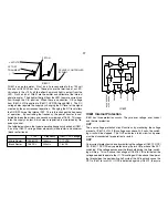
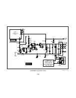
Page 18: ...N Q601 keeps C610 from charging when it is ON As the initial inrush current begins to dissipate the voltage across R621 decreases When this voltage drops below 20 volts D608 turns OFF causing Q601 to turn OFF When Q601 turns OFF C610 begins to charge When the charge of C610 a 10 uf capacitor reaches about 14 volts D606 begins to conduct After this occurs the voltage drop across R621 becomes only a...

Page 19: ...T 77 20B Q601 C610 R622 D603 MTZJ T 77 33B C609 R618 VIN FROM C620 TO REGULATION IC601 1 OCP FB INRUSH CURRENT PROTECTION 24 AND ABOVE 3CTV27 1224 A BOARD R627 R628 AC HI FROM RY602 AC LO FROM T602 3 TO R637 SWITCHING SUPPLY SWITCHING B TO T603 5 PRT REGULATION FROM IC602 2 135V R626 R645 R619 R605 R606 PH601 PC123FY2 1 2 4 3 ...

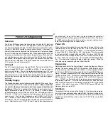
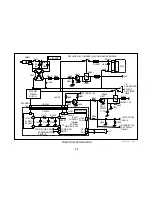
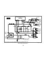
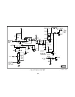
Page 20: ...cle the FET is turned OFF and current stops flowing through T603 4 and 5 and T603 2 and 3 This switching ON and OFF of the internal FET whose Drain and Source are IC601 3 and 2 respectively produces a signal output at T603 7 that is rectified by D613 and applied to IC601 4 VIN The DC voltage produced by D613 is used to sustain the input voltage at IC601 4 VIN When this sustaining voltage is missin...

Page 21: ...32 R641 R633 C619 D611 R643 C652 R646 D614 D613 R638 CREATES AUDIO B CREATES LOW B T603 CREATES 135 FROM 135 ERROR FROM IC602 2 PH601 PC123FY2 4 3 1 2 R645 R644 IC601 STR F6624 6654 CONVERTER D GND VIN OCP FB 3 5 2 4 1 S 7 8 2 3 5 4 16 17 14 13 11 12 A BOARD C620 ONLY FOUND IN 24 AND ABOVE MODELS SEE IN RUSH CURRENT PROTECTION IN RUSH CURRENT PROTECT FROM Q602 Q603 123 7 VDC 122 8 VDC ...

Page 22: ...ximum white raster and minimum black raster loads 135 Frequency IC601 1 DC Voltage White Raster 135 6 DCV 145kHz 1 71 VDC Black Raster 136 DCV 200kHz 1 6 VDC OSC UVLO OVP TSD LATCH 1 3 4 5 FDBK OCP 2 Vin OVER CURRENT FEEDBACK SOURCE DRAIN SUPPLY GROUND IC601 IC601 Internal Protection IC601 has three protection circuits They are over voltage over current and thermal protection OVP The over voltage ...

Page 23: ...32 R641 R633 C619 D611 R643 C652 R646 D614 D613 R638 CREATES AUDIO B CREATES LOW B T603 CREATES 135 FROM 135 ERROR FROM IC602 2 PH601 PC123FY2 4 3 1 2 R645 R644 IC601 STR F6624 6654 CONVERTER D GND VIN OCP FB 3 5 2 4 1 S 7 8 2 3 5 4 16 17 14 13 11 12 A BOARD C620 ONLY FOUND IN 24 AND ABOVE MODELS SEE IN RUSH CURRENT PROTECTION IN RUSH CURRENT PROTECT FROM Q602 Q603 123 7 VDC 122 8 VDC ...

Page 24: ...s connected for operation to restart Operating the Supply without a Load It is important to be able to isolate whether a problem is in the power supply or other circuitry This supply can be run unloaded at AC input voltages ranging from 30VAC to 120VAC You can unload the supply by unsoldering one side or removing L603 After removing L603 place a jumper across the contacts of RY602 Plug the set int...

Page 25: ...32 R641 R633 C619 D611 R643 C652 R646 D614 D613 R638 CREATES AUDIO B CREATES LOW B T603 CREATES 135 FROM 135 ERROR FROM IC602 2 PH601 PC123FY2 4 3 1 2 R645 R644 IC601 STR F6624 6654 CONVERTER D GND VIN OCP FB 3 5 2 4 1 S 7 8 2 3 5 4 16 17 14 13 11 12 A BOARD C620 ONLY FOUND IN 24 AND ABOVE MODELS SEE IN RUSH CURRENT PROTECTION IN RUSH CURRENT PROTECT FROM Q602 Q603 123 7 VDC 122 8 VDC ...

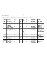
Page 26: ...or IC501 Pin and OCP 5 4 clicks Power ON Degauss ON and OFF and Shutdown No No 4 No Set ON and symptom repeats IC604 5 Volt Regulator Data problem 9 4 clicks Power ON Degauss ON and OFF and Shutdown No No 4 the fourth flash stays on for several seconds No Set ON and symptom repeats IC603 9 Volt Regulator IC1301 YCJ or IC301 Depending on model Audio B 3 Normal Yes No Normal Yes Set turns OFF PS401 ...

Page 27: ...22 NOTES ...

Page 28: ...normally The voltage at IC501 6 is proportional to the High Voltage If the High Voltage becomes excessive the voltage at IC501 5 will become greater than that at IC501 6 This would cause IC501 7 to output a HIGH This HIGH voltage activates the Latch Note This is a departure from the way previous models have worked Typically when the H pro tect circuit was activated it turned ON a transistor that g...

Page 29: ...CTV27 1225 TO POWER RELAY RY602 R559 D520 A BOARD C546 D519 R548 D518 RD8 2ES D517 R561 135 STANDBY 7 5V R663 Q604 R642 RELAY FROM IC1001 8 MB BOARD VIA CN2002 7 STANDBY 7 5V Q505 C534 R557 R555 D516 R554 R556 R553 135 C551 R568 PART OF T505 FBT 4 Q502 H DRIVE FROM T501 6 HDT 1 2 L510 200V R508 HLDWN TO IC1001 35 MB BOARD R655 R656 Q608 D619 MTZJ T 77 10B ...

Page 30: ...nal is output from the IC1301 11 E W and applied to the Pin Out circuit This signal is compared with the HP signal to create a Pulse Amplitude Modulated signal that is applied to the Horizontal circuit The purpose of this signal is to create a uniform picture width on the screen Vertical The vertical drive signals are generated by the YCJ after it successfully completes initial communication with ...

Page 31: ...ENT AND LINEARITY IC502 V OUT 3 34 33 11 13 14 1 2 4 3 5 6 DF QP DRIVE 5 12V 15V 27 32 ONLY NECK ASSEMBLY ABL IN HD HP EW VD VD IC1301 Y C J HV G2 FOCUS H DY H DY V DY V DY DEFLECTION BLOCK 9CTV27 1227 H OUT Q502 MB BOARD A BOARD D BOARD VA BOARD QP OUT FBT T505 HEATER 200V CN601 ...

Page 32: ...se sets it is the HP H OFF line In these models during an H protect condition pin 18 would be grounded and HD at pin 19 would be halted The H protect circuit does not operate in this manner in the BA 5 chassis but should IC1301 18 HP be grounded it would cause HD to cease IC1301 18 HP should be checked for a short to ground in the event that the YCJ is not outputting HD If IC1301 YCJ is outputting...

Page 33: ...135V T505 1 2 FLYBACK TO 2nd ANODE MAIN HP DY R383 R385 9V B 135V R547 R502 R509 HD HORIZONTAL DEFLECTION 7CTV27 1226 FROM PIN OUT Q504 T501 HDT ABL G2 CN501 4 21 00 9V R548 D509 R516 C502 33 44 11 FV SV HV FOCUS H SIZE AND LINEARITY CIRCUIT THIS CIRCUIT DIFFERS DEPENDING ON CRT SIZE 18 HP IC1301 CXA2131AS Y C J MB BOARD A BOARD ...

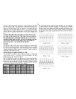
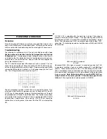
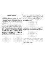
Page 34: ...ked These resistors are 47 ohms and should always be checked with an ohmmeter because they have a ten dency to change value when subjected to heat They should never read much higher than 47 ohms with an ohmmeter Next check the signals at IC502 1 and 7 They should look like the wave forms shown below If these signals are missing check IC1301 13 and 14 If these signals are not present check the data...

Page 35: ...8172 VERT OUT 15v D510 C541 R384 R517 R518 R540 R519 CN501 R538 R387 R536 VD 2 R539 C543 R549 D513 R550 D514 4 20 00 15V SCAN DERIVED SUPPLY FROM T503 7 R541 5 6 DY 13 14 35 34 33 SCL SDA 5 VTIM MAIN VP 9V 44 A BOARD MB BOARD VD I PROTECT TO CN003 5 MB BOARD FROM T503 9 12V SCAN DERIVED SUPPLY ...

Page 36: ...d by IC1001 Control Tuning System for V Chip and Closed Captioning and by IC1302 Digital Comb Filter Digital Comb Filter The Digital Comb Filter is used when composite video inputs are used The composite video signal output at IC1301 6 is buffered and filtered by Q1311 Q1312 FL1301 and Q1310 You should note that the chroma signal has a very low amplitude at FL1303 The signal is then input to IC130...

Page 37: ...M J202 FRONT A V J201 CN2009 CN1004 IC1304 NJM2534M VIDEO SW IK R OUT B OUT G OUT Y1 C1 IC1301 Y C J CXA2131AS CN2001 CN1001 CN2002 CN1003 VIDEO PATH 24 AND UNDER 4 24 00 6CTV27 1223 A BOARD IC1302 TC90A49P DIGITAL COMB FILTER 14 13 17 CKIN AIN COUT 20 Q1313 Q1354 FL1302 A1306 1307 1308 MB BOARD 7 20 19 17 7 X1001 8MHz 6 41 TO A BOARD FOR AUDIO SWITCH 20 19 17 IK RETURN FROM Q1331 C TO Q1317 R BUF...

Page 38: ...rea that appears to be one pulse Expand it and you will see that there are three distinct pulses one for each color Your scope should be set to 5ms per division Some scopes that have less than 100MHz bandwidth may have trouble triggering on these signals Once the IK detect circuit in the YCJ detects that the proper current is flowing to each cathode the video is unblanked and a picture may be seen...

Page 39: ...718 HEATER R714 RV701 HSTAT R715 FOCUS R716 G2 9 8 R708 R712 R713 R711 R709 R710 7 6 VCC D701 D702 D703 CN706 CN502 200V FROM D511 IC1301 CXA2131AS YCJ 23 R1395 R1376 Q1316 24 R1394 R1375 Q1315 22 R1378 Q1317 R1396 R OUT B OUT G OUT R1392 Q1350 Q1331 R1393 R1391 21 R1397 IKIN D1310 UDZ TB 17 5 AB 9V 6 6 35 34 SDA SCL TO Q1336 AFC BUFFER 9V R1379 R1381 R1380 RGB EXPANDED CB BOARD MB BOARD ...

Page 40: ...d be flashing in se quences of two or four If a problem occurs with one of the colors the set will remain in video blanking mode This means no video or OSD will be displayed However the YCJ will continue to output these IK pulses One possible method for seeing these lines uses the Service Mode You can enter Service Mode by pressing Display 5 Vol then Power After the set is ON press the 1 button 15...

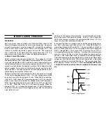
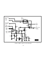
Page 41: ...718 HEATER R714 RV701 HSTAT R715 FOCUS R716 G2 9 8 R708 R712 R713 R711 R709 R710 7 6 VCC D701 D702 D703 CN706 CN502 200V FROM D511 IC1301 CXA2131AS YCJ 23 R1395 R1376 Q1316 24 R1394 R1375 Q1315 22 R1378 Q1317 R1396 R OUT B OUT G OUT R1392 Q1350 Q1331 R1393 R1391 21 R1397 IKIN D1310 UDZ TB 17 5 AB 9V 6 6 35 34 SDA SCL TO Q1336 AFC BUFFER 9V R1379 R1381 R1380 RGB EXPANDED CB BOARD MB BOARD ...

Page 42: ...mponents separated IC302 Digital Comb Filter or the B board can do this The B board is only used on the KV27FV16 model and contains a 3D Comb Filter Whichever comb filter is used they will have the same effect on the signal path They each take com posite video input and output separated Y and C These Comb Y and Comb C signals are then re input to the YCJ at pins 22 and 20 respec tively Y C Process...

Page 43: ...N2006 C348 C359 C361 C322 C312 CN305 TO R BUFFER Q389 TO G BUFFER Q388 TO B BUFFER Q387 YI IN CI IN CVBSI IN CVBS4 IN DVDY IN CVBS3 IN Y2 IN DVDCR IN DVDCB IN CVBS2 IN C2 IN C OUT MON OUT FSC OUT COMB C COMB Y PIP OUT PIP CBIN PIP CRIN PIP YIN YUVSW R OUT G OUT B OUT 7 7 VIDEO PATH 27 AND ABOVE 10CTV27 1229 C325 19 59 20 24 48 22 47 46 45 17 1 2 3 39 37 Q349 Q359 FL301 Q358 1 3 5 HA BOARD MA BOARD...

Page 44: ...amp is in the rear and the headphone jack is in the front of the A board The signal then passes through the headphones and back to CN407 If there are headphones plugged into the headphone jack J401 the audio will not be returned back This may be useful for troubleshooting in the event of a bad headphone jack The back signal to CN407 is then applied to the R or L speaker terminal depending on which...

Page 45: ...L SPK L R BACK R GO L BACK L GO HP GND TO CN408 SPR SPL 2 1 2 3 4 5 R BACK R GO L BACK L GO HP GND TO CN407 CN406 CN407 J401 HEADPHONE CN408 R427 C438 R428 C439 AUDIO B FROM L601 C420 C421 R436 R437 R438 R439 J202 CN2002 TO CN1004 MB BOARD R446 R442 Q410 R441 R440 C441 C442 Q411 R445 R447 D401 12V R237 C216 C210 R238 CONTROL LINES TO IC1405 2 4 CN2009 O VOL FROM IC1001 3 VIA CN1003 MB BOARD S0 S1 ...

Page 46: ...essing is per formed The left and right signals are output for the Var Fix Output at J402 on the A board from IC404 12 and 29 The customer can select from the menu if they want this output to be fixed or variable The outputs from IC404 13 and 28 are the main audio outputs of the set Depending on the model this audio will be input to IC403 SRS or to the A board for amplification If the model contai...

Page 47: ... AUX0 AUX1 OUTB OUTA LINE B LINE A MON B MON A SDA SCL IC404 AUDIO PROCESSOR NJW1130G C448 R405 C447 R404 R403 R406 C201 R407 C202 R408 C450 C451 CN460 CN451 MODE1 MODE2 LIN RIN ROUT LOUT IC403 SRS NJM2198 1 2 4 3 OUT IN1 IN2 IN3 IN4 MUTE R OUT TO CN407 L OUT TO CN407 MUTE FROM SYSCON IC1001 5 VIA CN2002 9 IC402 AUDIO AMP TDA8580Q R436 R437 R439 C420 C421 C460 C458 CN450 CN460 TV L TV R VI L VI R ...

Page 48: ...APPENDIX ...
Page 49: ...n current flows through the winding between T621 1 and T621 3 The voltage is not permanent due to C630 As C630 charges it reduces the voltage at Q621 G Once this voltage falls below a certain threshold Q621 Converter turns OFF Once Q621 Converter turns OFF all polarities are reversed This rever sal of polarity helps speed up turn OFF of Q621 D623 along with C631 and R640 form a snubber network vol...

Page 50: ... SIDE R631 R636 Q622 PROT C699 C630 R632 D698 D624 D699 MTZ T 77 15 R633 R634 D626 RD6 2ESB2 C635 R638 C633 D627 C636 T621 SRT D628 C637 G BOARD IC622 5V REG BAO5T CN641 C650 I O G STANDBY 5V TO A BOARD CN1641 TO RY600 POWER RELAY 6 5 4 3 2 1 11 10 9 8 STANDBY SUPPLY 3 CTV26 1187 10 D D625 S 7 2VDC TO Q646 E BACKUP 12 28 99 ...

Page 51: ...r Secondary Output The power coupled through T621 SRT places a voltage on T621 9 that when rectified and filtered by D628 and C637 is 7 2 volts This voltage is constant due to the regulation circuit on the primary side of T621 SRT This 7 2 volts is applied to Q646 E for backup during the start of regula tion by the regular power supply It is also applied to IC622 5 Volt Regulator which regulates i...

Page 52: ... SIDE R631 R636 Q622 PROT C699 C630 R632 D698 D624 D699 MTZ T 77 15 R633 R634 D626 RD6 2ESB2 C635 R638 C633 D627 C636 T621 SRT D628 C637 G BOARD IC622 5V REG BAO5T CN641 C650 I O G STANDBY 5V TO A BOARD CN1641 TO RY600 POWER RELAY 6 5 4 3 2 1 11 10 9 8 STANDBY SUPPLY 3 CTV26 1187 10 D D625 S 7 2VDC TO Q646 E BACKUP 12 28 99 ...

Page 53: ...S SEL Service Company A Division of Sony Electronics Inc 1 Sony Drive Park Ridge New Jersey 07656 CTV270500 Printed in U S A ...

Reviews: