background image

23

DVP-CX995V

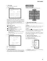
0-3. Peripheral

(3-2) Flash Rom

Data delete 

t

 write 

t

 read, and accord check

Error 32: Delete error
Error 33: Write error
Error 34: Read data discord
Error may occur due to defect of access with the CPU (MB
board IC205).

(3-3) SA-CD Check

Data write 

t

 read, and accord check

Error 36: Write/read data discord
Check for SA-CD circuit (MB board IC401 and around
circuit).

(3-4) Venc Check

Register write 

t

 read, and accord check

Error 37: Write/read data discord
Error may occur due to defect of access with the CPU (MB
board IC205).

(3-7) PROV Check

Data write 

t

 read, and accord check

Error 39: Write/read data discord
External RAM check for I/P converter (AV board IC401)
too.

(3-8) HDMI Check

Register write 

t

 read, and accord check

Error 43: Write/read data discord
Error may occur due to defect of access with the HDMI
transmitter (AV board IC600).

0-4. Servo

(4-2) Servo (F/E) Check

Data write 

t

 read, and accord check

Error 41: Read data discord
0x9249, 0x2942 and 0x4294 are written to the RAM address
0x602 of the DVD interface (front-end) (MB board IC104)
and then read for checking.

0-5. Video

(5-2) Interlace

Error: Not detected.
The command is transferred to the video D/A converter (AV
board IC500), and change the video signal to interlace.

(5-3) Progressive

AVD color bar command write 

t

 Video (Composite, Y/C)

OUT
Error: Not detected.
The command is transferred to the video D/A converter (AV
board IC500), and change the video signal to progressive.

(5-4) Color Bar

Error: Not detected.
The command is transferred to the video D/A converter (AV
board IC500), and the color bar signals are output from video
terminals.

0-6. Audio

Not used.

1. Drive Auto Adjustment

DVD reference disc:

Single Layer

TDV-520CS0 (J-2501-236-A) (NTSC)
HLX-503 (J-6090-069-A) (NTSC)
HLX-504 (J-6090-088-A) (NTSC)

Dual Layer

TDV-540C (J-2501-235-A) (NTSC, Opposite)
HLX-501 (J-6090-071-A) (NTSC)
HLX-505 (J-6090-089-A) (NTSC)

CD reference disc:

LUV-P01 (4-999-032-01)
YEDS-18 (3-702-101-01)
PATD-012 (4-225-203-01)

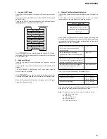
On the Test Mode Menu screen, press 

[1]

  key  on the remote

commander, and the drive auto adjustment menu will be displayed.

## Drive Auto Adjustment ##

Adjustment Menu

0. ALL (DL:Parallel)

1. DVD-SL

2. CD

3. DVD-DL (Parallel)

4. ALL (DL:Opposite)

5. DVD-DL (Opposite)

9. CLEAR DATA

Exit: RETURN

Normally, 

[0]

 or 

[4]

 is selected to adjust DVD (single layer), CD,

and DVD (dual layer) in this order. But, individual items can be
adjusted for the case where adjustment is suspended due to an error.
In this mode, the adjustment can be made easily through the
operation following the message displayed on the screen. Which
disc is currently adjusted is displayed on the fluorescent display
tube.

1-0. ALL (DL: Parallel)

Select 

[0]

 and press the 

[ENTER]

 key. Then, [1] DVD-SL disc, [2]

CD disc, and [3] DVD-DL (Parallel) disc are adjusted in this order.
Because the changer model can accept multiple discs in advance of
adjustment, adjustments can be continued by exchanging discs
automatically whenever an adjustment is completed following the
instruction on screen. You can exit the adjustment by pressing
the

x

button. In adjusting each disc, the mirror time is measured

to check the disc type. In the auto adjustment, whether the disc type
is correct is not checked unlike conventional models, and
accordingly, take care not to insert a different type of disc.

Three kinds of discs can be set in advance. In this case, set discs in
order to the displayed number with following the massage. Every
time after adjusting a disc, the disc is replaced and adjustment is
continued automatically.

Set Disc
Disc slot number 1: DVD-SL (TDV-520CS0 or HLX-503 or HLX-

504)

Disc slot number 2: CD (LUV-P01 or YEDS-18 or PATD-012)
Disc slot number 3: DVD-DL (TDV-540C or HLX-501 or HLX-

505)

Summary of Contents for DVP-CX995V Operating Instructions (DVP-CX995V CD/DVD Player)

Page 1: ... 003 Dynamic range DVD VIDEO Super Audio CD 103 dB CD 99 dB Wow and flutter Less than detected value 0 001 W PEAK Outputs Jack name Jack type Output level Load impedance LINE OUT AUDIO L R 1 2 Phono jack 2 Vrms 10 kilohms DIGITAL OUT OPTICAL Optical output jack 18 dBm wave length 660 nm DIGITAL OUT COAXIAL Phono jack 0 5 Vp p 75 ohms HDMI OUTPUT TypeA 19 pin 5 1CH OUTPUT Phono jack 2 Vrms 10 kiloh...

Page 2: ...R DOTTED LINE WITH MARK 0 ON THE SCHEMATIC DIAGRAMS AND IN THE PARTS LIST ARE CRITICAL TO SAFE OPERATION REPLACE THESE COMPONENTS WITH SONY PARTS WHOSE PART NUMBERS APPEAR AS SHOWN IN THIS MANUAL OR IN SUPPLEMENTS PUBLISHED BY SONY SAFETY CHECK OUT After correcting the original service problem perform the following safety check before releasing the set to the customer Check the antenna terminals m...

Page 3: ...tion 2 7 47 7 10 Schematic Diagram MB Section 3 7 48 7 11 Schematic Diagram MB Section 4 7 49 7 12 Schematic Diagram MB Section 5 7 50 7 13 Schematic Diagram MB Section 6 7 51 7 14 Schematic Diagram MB Section 7 7 52 7 15 Schematic Diagram AV Board 1 5 53 7 16 Schematic Diagram AV Board 2 5 54 7 17 Schematic Diagram AV Board 3 5 55 7 18 Schematic Diagram AV Board 4 5 56 7 19 Schematic Diagram AV B...

Page 4: ...When replacing the mounted MB board A 1132 163 A since the adjustment value is not set up correctly Drive Auto Adjustment in the Test Mode can t be performed In this case initialize memory in the following procedures Procedure 1 Connect a video monitor to VIDEO LINE OUT jack J103 2 Press the TOP MENU CLEAR I 1 keys on the remote commander RM ASP001 in this order with standby status to enter the Te...

Page 5: ...ded in VR mode Video Recording format Copy Once programs recorded on CPRM compatible DVD Rs An 8 cm disc The 12 cm disc adapter should not be used for 8 cm discs because it may cause the disc to jam or the player to malfunction CPRM Content Protection for Recordable Media is a coding technology that protects copyright for Copy Once programs Notes Notes about DVD RWs DVD Rs DVD RWs DVD Rs or CD Rs ...

Page 6: ...cable AV board to PANEL L board cables MB board to DRIVER board SENSOR board cable MB board to LED board ALIGNMENT OF GEAR CAM PHASE WITH DOOR ASS Y CLEANING OF OPTICAL PICK UP door assy gear cam Align a slit of door assy with a marking on the bottom land of gear tooth when the gear is rotated fully in arrow direction as shown optical pick up pulley assy Remove the pulley assy and clean the lens o...

Page 7: ...les cables When installing the cables it is made to make it crawl in a chassis AV board AV board cables It is made to contact and for there not to be a switching regulator and cables switching regulator MB board switching regulator ...

Page 8: ...8 DVP CX995V SERVICE POSITION MB board Optical pick up block MB board CN303 Connect the jig J 2501 199 A to MB board CN303 and PANEL L board CN1003 PANEL L board CN1003 optical pick up block DVBU65 ...

Page 9: ...l discs mode Lights up when the player outputs progressive signals Disc type Playing time Playing status Current play mode All discs mode Current disc Current scene Playing time Disc type Current track CD Super Audio CD VIDEO CD or album DATA CD Lights up when playingMP3 audio tracks Playing status Current disc Current play mode All discs mode Current index CD Super Audio CD VIDEO CD or track DATA...

Page 10: ...BASE DOOR ASSY Page 15 3 12 DC MOTOR DOOR M603 Page 16 3 13 HOLDER TABLE SENSOR 400 Page 16 3 14 D SENS OUT BOARD D SENS IN BOARD Page 17 3 15 POP UP 400 ASSY Page 17 3 16 DOOR SW BOARD Page 18 3 17 LOCK SW BOARD LOADING SW BOARD Page 19 3 18 CD DVD MECHANISM DECK BLOCK CDM62 DVBU65 Page 20 3 19 MOTOR 400 ASSY LOADING M602 TABLE M601 LOADING MOTOR BOARD Page 20 3 20 OPTICAL TRAVERSE UNIT DBU 3 Pag...

Page 11: ...two screws case 3 TP2 5 case 4 two screws case 3 TP2 1 two screws case 3 TP2 qs MB board 8 two screws BVTP3 8 9 two harnesses 1 wire flat type 25 core CN303 7 connector CN304 6 connector CN305 2 flat type wire 31 core CN101 5 flat type wire 29 core CN501 4 flat type wire 33 core CN205 3 tape 0 two screws BVTP3 8 qa connector CN203 ...

Page 12: ... 1 flat type wire 31 core CN101 7 2 eight screws BVTP3 8 3 screw BVTT3 8 0 connector CN304 qa connector CN303 qs connector CN302 qd connector CN301 qf AV board 6 harness 5 screw BV3 3 4 AV BOARD 3 5 BRACKET L R 4 screw BVTP3 8 3 two screws BVTP3 8 1 two screws BVTP3 8 5 bracket R 2 bracket L ...

Page 13: ...ont panel section 1 five screws BVTP3 8 3 two screws BVTP3 8 2 screw BVTP3 8 5 claw 4 claw 1 screw BVTP3 8 3 cover PT 2 screw BVTP3 8 8 three screws BVTP3 8 4 six screws BVTP3 8 5 three screws BVTP3 8 6 cover CDM 7 bracket shield double faced tape 9 bracket CDM ...

Page 14: ...sher 0 8 washer 2 screw BVTP3 8 9 DVBU65 assy 4 screw BVTP3 8 3 8 DVBU65 ASSY 3 9 SWITCHING REGULATOR Note When installing the rear panel tighten three screws first in following the order 1 screw BVTP3 8 3 rear panel block 7 switching regulator 6 two screws BVTP3 8 4 connector CN101 5 screw BVTP3 8 2 two screws BVTP3 8 rear panel 1 2 3 ...

Page 15: ...OOR ASSY 1 screw M3 14 2 guide door 3 table 400 assy 4 10 washer Note When installing the guide door align the positions as shown 2 three screws BVTP3 8 1 connector CN904 3 cover table 4 door assy 5 two screws BVTP3 8 6 eight screws BVTP3 8 7 base door assy ...

Page 16: ...TABLE SENSOR 400 1 belt 400 4 DOOR MOTOR board 5 DC motor door M603 3 Remove two solders 2 two screws BVTP3 8 1 four screws BVTP3 6 4 SENSOR board 5 screw PTTWH3 6 2 connector CN83 3 two connectors CN81 CN82 6 two claws 7 holder table sensor 400 6 claw ...

Page 17: ...OUT BOARD D SENS IN BOARD 3 15 POP UP 400 ASSY 5 screw PSW3 8 6 D SENS OUT board 1 screw PTTWH3 6 2 clamp 8 D SENS IN board 3 two step screws T1 4 bracket sensor 400 7 screw PSW3 8 1 screw PTPWH3 6 2 step screw 3 pop up 400 assy ...

Page 18: ... illustration and rotate it fully in the direction of the arrow B 3 When the gear cam happens to go too deep return it to the original position in the direction of the arrow C 4 gear B 2 gear cam 6 DOOR SW board C B A lever pu joint two rotary switches slider pop up gear cam DOOR SW board The levers of the two rotary switches on the DOOR SW board are shown in the illustration below Precaution duri...

Page 19: ...00 in the direction of the arrow B fully 2 screw BVTP3 8 5 screw BVTP3 12 4 belt 400 8 screw BVTP3 8 0 screw BVTP2 6 qa LOADING SW board 9 LOCK SW board 7 gear center 6 pulley 400 Note for installation When installing the LOADING SW board and LOCK SW boards align the leads position as shown LOADING SW board LOCK SW board leads position A B ...

Page 20: ... MOTOR BOARD 4 four screws BVTP3 8 3 screw PSW3 8 2 connector CN903 1 connector CN905 5 seven screws BVTP3 8 6 CD DVD mechanism deck block CDM62 DVBU65 4 motor 400 assy loading M602 1 two belts 400 3 Remove two solders 5 Remove two solders 2 three screws BVTP3 8 6 motor 400 assy table M601 7 LOADING MOTOR board ...

Page 21: ... the pick up may be damaged qd optical traverse unit DBU 3 8 step screw M qa insulator RB 9 step screw M qs insulator RB 3 flexible board CN0029 2 flat type wire 31 core CN003 1 Make solder land two points short on RF TRANSLATION board for prevent damage by static electricity DBU400 holder assy SL001 4 flexible flat cable CN001 5 screw BVTP2 6 6 RF TRANSLATION board 0 insulator RB 7 step screw M ...

Page 22: ...key on the remote commander and the following check menu will be displayed BackEnd Diagnosis Check Menu 0 Quit 1 All 2 Version 3 Peripheral 4 Servo 5 Video 6 Audio Model DVP CX995V Revision x xxx 0 0 Quit Quit the Syscon Diagnosis and return to the Test Mode Menu 0 1 All All items continuous check This menu checks all diagnostic items continuously Normally all items are checked successively one af...

Page 23: ...NTSC HLX 504 J 6090 088 A NTSC Dual Layer TDV 540C J 2501 235 A NTSC Opposite HLX 501 J 6090 071 A NTSC HLX 505 J 6090 089 A NTSC CD reference disc LUV P01 4 999 032 01 YEDS 18 3 702 101 01 PATD 012 4 225 203 01 On the Test Mode Menu screen press 1 key on the remote commander and the drive auto adjustment menu will be displayed Drive Auto Adjustment Adjustment Menu 0 ALL DL Parallel 1 DVD SL 2 CD ...

Page 24: ...ode DVD ON 4 Focus Error Check 5 Focus ON 6 Spindle Start 7 Tracking Error Level Adjust 8 Tracking Error Offset Adjust 9 Tracking ON 10 RF Level Adjustment 11 Spindle Calibration 12 Tracking Off 13 Tracking Error Level Adjust 2nd 14 Tracking Error Offset Adjust 2nd 15 Tracking ON 16 Auto Focus Gain Adjust L0 17 Auto Tracking Gain Adjust L0 18 Sled ON 19 CLV ON 20 Auto Focus Balance Adjust L0 21 Au...

Page 25: ...in advance In this case set discs in order to the displayed number with following the massage Every time after adjusting a disc the disc is replaced and adjustment is continued automatically Set Disc Disc slot number 1 DVD SL TDV 520CS0 or HLX 503 or HLX 504 Disc slot number 2 CD LUV P01 orYEDS 18 or PATD 012 Disc slot number 3 DVD DL TDV 540C only 1 5 DVD Dual Layer Disc Opposite Note Make sure u...

Page 26: ...spindle servo 5 Track Turn on off the tracking servo 6 Sled Turn on off the sled servo 8 Focus Ramp In the laser diode on and focus servo off status repeat the focus up down 2 4 Track Layer Jump 4 Track Layer Jump 1 1Tj FWD 2 1Tj REV 3 200Tj FWD 4 200Tj REV 5 2kTj FWD 6 2kTj REV 9 Lj L1 L0 FWD 0 Lj L0 L1 REV Exit RETURN On this screen track jump etc can be performed Only for the DVD DL the focus j...

Page 27: ...d in out 0 Off 1 On Door open close Poper up down Disc Sensor Indicates sensitivity of the disc sensor The value is raging from 0 to 3FF 2 6 Memory Check The display image is shown below and three screens in total can be selected 6 Memory Check Flash Data 1 CD SL L0 L1 An Off A xx xx xx xx An Off B xx xx xx xx An Off C xx xx xx xx An Off D xx xx xx xx An Off E xx xx xx xx An Off F xx xx xx xx An G...

Page 28: ...the screen PAUSE Enters the Table Sensor Adjustment Mode Mecha Adjust The 400CHG Mecha Adjust appears on the screen Display when PLAY is selected in the Changer Mecha Check Note Refer to page 32 for TABLE SENSOR ADJUSTMENT 400CHG Table Rotate RIGHT Turn Right LEFT Turn Left Table 1 2 3 4 X X X X Disc Sensor XXX RETURN Exit RIGHT 1 Rotates table counterclockwise Turn Right LEFT 1 Rotates table cloc...

Page 29: ... IC205 on the MB board F E IC104 on the MB board 6 Video Level Adjustment On the Test Mode Menu screen selecting 6 displays color bars for video level adjustment During display of color bars OSD disappears but the menu screen will be restored if pressing the RETURN key DISPLAY SECTION DISPLAY TEST MODE Execute the Self Check Mode along the following flow 1 Entering the Display Test Mode The Displa...

Page 30: ... 0 4 sec interval 0 4 sec interval 0 4 sec interval ALL GRIDs light up 0 2 sec interval GRID2 on Wait for SIRCS code receiving Once the SIRCS code is received the check finishes Cancel processing Press the DISC AMS knob SIRCS reception check SIRCS reception check finish 6 Key Check After the SIRCS reception check finished the Key check is executed Upon start of the Key check KEY CHECK is displayed...

Page 31: ...this time even if a signal from a key on the set remote commander or keyboard is received nothing changes At the SIRCS reception check Key check Jog and LED check and Keyboard check if you proceed to the next check without completing current check the check name that has not completed yet is displayed instead of TEST OK as follows If SIRCS reception check has not completed SIRCS NG If JOG dial is ...

Page 32: ...ons in this mode Q key Loading mechanism IN operation q key Loading mechanism OUT operation w key Pop up part UP operation W key Pop up part DOWN operation TABLE SENSOR ADJUSTMENT After the Pop Up Mechanism Adjustment perform this adjustment continuously 1 Loosen the fixing screw Moving the holder little by little stop it at a boundary point where the PROGRESSIVE LED blue goes off and the SA CD LE...

Page 33: ...74 to FF 54 to FF FE S L1 54 to FF VTS2 00 to 10 TE levDVD 28 to 48 28 to 48 28 to 48 TE levCD 34 to 60 TE Offset D0 to FF A0 to CC 20 to E0 20 to E0 00 to 30 00 to 30 00 to 30 FCS Gain 20 to 3F 18 to 38 20 to 48 20 to 48 TRK Gain 30 to 50 30 to 50 30 to 50 30 to 50 FCS Bal 1 FCS Bal 2 36 to 4F 36 to 4F 36 to 4F 36 to 4F REFQ1 REFQ2 0C to 30 14 to 24 0C to 30 0C to 30 Jitter 07 to 14 07 to 0F 07 t...

Page 34: ...o LevelAdjustment so that color bars are generated 2 Confirm that the S Y level is 1 0 0 05 Vp p Fig 6 3 6 3 2 Progressive Video Output Level Adjustment Purpose This adjusts progressive video output level If it is incorrect correct brightness will not be attained when connected to for instance projector Mode Video level adjustment in test mode Signal Color bars Check point COMPONENT VIDEO OUT Y co...

Page 35: ...oscope Specification 700 50 mVp p Checking method 1 In the Test Mode Menu select the 6 Video LevelAdjustment so that color bars are generated 2 Confirm that the B Y level is 700 50 mVp p Fig 6 6 6 3 7 Checking Component Video Output R Y Purpose This checks component video output R Y If it is incorrect correct colors will not be displayed when connected to for instance projector Mode Video level ad...

Page 36: ...rection 5 Turn the RV301 on MB board and adjust so that the H portion A of DSENS_OUT waveform is twice the width of the H portion B of HH_OUT waveform Adjustment Location MB board 6 Loosen the fixing screw move the mounting board SENSOR and secure the mounting board SENSOR at the point the H portion of the HH_OUT waveform comes the center of the H portion of the DSENS_OUT waveform DSENS_OUT HH_OUT...

Page 37: ...DVP CX995V 37 37 DVP CX995V CN301 RV301 Disc Detect Sensor Adjustment MB Board Side A 3 1 Adjustment Location ...

Page 38: ...ADR 7 29 36 38 45 DQ0 DQ14 DQ15A 1 25 16 10 1 48 A1 A21 W 11 G 28 E 26 RP 12 FLASH MEMORY IC202 CPU CE 1 132 RESET 124 CPU CE 3 134 CPU OE 117 CPU BE 0 128 CPU CE 2 133 DAC PCMCLK 55 SPDIF OUT 57 SCLK 208 SO 207 ADAC_CS 22 VIDEO_RST 9 IRQ 1 126 SQUEEZE 191 YC_CLKOUT VIDEO_RST H_INT_B SQUEEZE YC_CLK DIGITAL VIDEO SPDIF SACD DAC PCMCLK SACD I2S YC0 YC7 YC0 YC7 3 IRQ 2 125 CPU WAIT 131 CPU RW 130 IF_...

Page 39: ...ODE_SW 83 BE_CS 23 BE_BUSY BE_RXD0 BE_TXD TMODE_SW BE_CS BE_BUSY 33 G RFSACD A AUD_CLK 29 SA_SYS_CLK L BE_A_MUTE P CPU I F N VMUTE R BE_RST J CCLK SCL 19 CDTI SDA 20 CSN CAD1 21 LRCK 17 BICK 9 DSDL1 25 DSDR1 26 DSDL3 29 DSDR3 30 DSDL2 27 DSDR2 28 DSDL4 23 DSDR4 24 DCLK 22 PCM 5 1CH SDTI1 14 MCLK 10 SDTI2 16 SDTI3 15 SDTI4 SCLK SO ADAC_CS DAC LRCK DAC SCLK FLFR CSW SLSR DLDR 13 D DAC E DAC PCMCLK F...

Page 40: ..._2 CSCL 43 33 RESET8 22 SCL 21 SDA BE_SCL BE_SDA VIDEO_RST I2C DIGITAL_VIDEO SIGNAL PATH VIDEO COMPOSITE Y C PLAY VIDEO YUV PLAY AUDIO COMPONENT VIDEO VIDEO LEVEL RV501 35 RSET2 59 CLKO 5 SDA 6 SCL PROGRESSIVE VIDEO OUTPUT LEVEL RV500 J102 1 2 3 4 5 6 7 8 COMPONENT VIDEO OUT J600 HDMI OUT Y PR CR PB CB VIDEO LINE OUT J103 2 2 1 2 S VIDEO OUT J101 1 2 29 31 WIDE ON OFF SWITCH Q103 104 DATA0 DATA0 1...

Page 41: ...RIVE IC961 1 2 WAKE UP SWITCH IC302 305 REMOTE CONTROL RECEIVER IC1002 LED DRIVE Q1001 1004 Q1006 Q1007 FLUORESCENT INDICATOR TUBE FL1001 FL DRIVER IC1001 SYSTEM CONTROLLER IC304 2 2 VDISP 30V 5V REGULATOR IC603 5V POWER HDMI OUT 7V REGULATOR IC103 BU DRIVER 7V TABLE MOTOR B SW 12V M SW 12V M 12V D F1 F2 MUTING B OPAMP B D301 RESET 16 P_CONT 70 PON_CHECK 95 DRM 47 AC IN Q306 Q305 CLOSE OPEN S611 D...

Page 42: ...ectrolytics and tantalums All resistors are in Ω and 1 4 W or less unless otherwise specified f internal component C panel designation A B Line B B Line H adjustment for repair Voltages and waveforms are dc with respect to ground under no signal conditions no mark DVD PLAY SACD PLAY CD PLAY Impossible to measure Voltages are taken with aVOM Input impedance 10 MΩ Voltage variations may be noted due...

Page 43: ... PRINTED WIRING BOARD RF TRANSLATION Board See page 42 for Circuit Boards Location Uses unleaded solder CN003 CN001 CN002 1 863 815 11 11 RF TRANSLATION BOARD MB BOARD CN101 S OPTICAL TRAVERSE UNIT DBU 3 A B C D 1 2 3 4 SL001 Page 44 ...

Page 44: ... C216 C208 R1022 R1023 R1024 R1025 C204 R1033 R1034 R353 R354 CN304 R358 C142 R1055 RB206 RB202 RB203 RB205 C145 C146 C149 Q307 CN301 C203 C202 C201 CN303 X201 R1028 C153 R197 R196 R194 R185 R184 C154 R181 C155 R177 R176 R175 R174 R173 R170 R169 R168 R167 R166 R161 R165 R164 R163 R162 R160 R159 R158 R157 R154 R152 R149 R148 R143 C156 R141 R121 R114 R113 R112 R111 R107 R106 R105 R104 R103 R102 Q105...

Page 45: ...7 R298 R299 R300 R301 C104 C105 C106 C107 C108 C109 C110 C111 C115 C116 C117 C118 C179 C119 C120 C121 C122 C423 C422 C421 C419 R321 R326 R327 R328 R330 R331 R334 R366 R362 R361 R360 C322 C321 C320 R337 R338 R424 R342 R344 R345 R346 R348 R349 R350 R351 R352 C123 C249 C247 C246 C245 C244 C243 C241 C240 C239 C237 C236 R261 C125 C233 C232 C231 C128 C226 C130 C131 C132 C133 C217 C215 C214 C213 C212 C21...

Page 46: ... 3V 0 01 0 01 2 2 31P 100 6 3V 100k 22 6 3V 0 01 270 22 22 220 100k 22 6 3V 0 01 22 22 270 220 2SC4617FTLQ 22 6 3V 6 8k 1 1 1 5P 100 6 3V 22 6 3V 100 6 3V 100 6 3V 0 01 100 6 3V 0 01 1SS355 0 01 0 01 24P 9P 31P 10k 10k 0 01 4 7k 4 7k 0 01 100k 2SB1132 T100 QR 1000p 1000p B1 B2 B3 B4 B5 5V A 1 8V A AGND 1 8V D B_ERROR XBCLK XPCLK XDATA B_WCLK B_V4 FE_CLK RFSACD XERROR 3 3V A FE_RST BE_SCL BE_SDA FE...

Page 47: ...2k 0 01 0 01 LMV324MT NOPB 0 22 30k 4 7k 4 7k 4 7k LMV324MT NOPB 0 22 24k 1000p 27k 0 01 0 01 100p 100p 15k 56k 56k 22k 22 6 3V 33k 33k 10k 10k 6 8k 47k 47k 0 01 0 01 0 01 100 10V BA07FP E2 47 6 3V 1k 10k 10k 0 01 0 01 47 16V 22 6 3V 4 7k B1 B2 B3 B4 B5 DGND 3 3V D 5V D PGND 12V D FACT TACT STEPA STEPB MUTE_DRV MUTE_SP TRK TRK FCS FCS SPDIR SP SP SLB SLB SLA SLA SP G O I 2 7 7V REGULATOR TRACKING ...

Page 48: ...7 47 0 01 10k 10k 10k 10k 0 01 22 6 3V 0 01 470p 0 01 10k 10k 10k 10k 0 01 10k 10k 10k 0 01 47 4V 0 01 47 4V 47 1M 1SS367 47 0 0 01 27MHz 4p 4p 47 10 10k 2 7k 1 8k 1 8k 10 10 10 10p 10p 10k 10k 10k 47 47 10 10 47 4V STE5588CVB 47 0 100p 100p 10k 0 0 01 0 01 0 0 0 0 SN74HCU04APWR 47 47 47 47 47 A1 A2 A3 A4 A5 A6 A7 A8 A9 BE_CS B_ERROR XBCLK XPCLK XDATA B_WCLK B_V4 FE_CLK DGND 3 3V D 1 8V D XERROR F...

Page 49: ...PCM_LRCK PCM_DATA3 PCM_DATA2 PCM_DATA1 PCM_DATA0 PCM_SCLK SO SCLK ADAC_CS BE_A_MUTE H_SDA_BP H_SCL_BP BE_SDA BE_SCL SACD_MCLK AUD_MCLK PCM_LRCK PCM_SCLK HDMI_MCLK YC_CLKOUT YC0 YC1 YC2 YC3 YC4 YC5 YC6 YC7 DQ0 DQ4 DQ15 DQ11 ADDR17 DATA15 DATA7 DATA14 DATA6 DATA13 DATA5 DATA12 DATA4 DATA11 DATA3 DATA10 DATA2 DATA9 DATA1 DATA8 DATA0 F_OE F_CE ADDR1 ADDR17 DATA15 DATA7 DATA14 DATA6 DATA13 DATA5 DATA12...

Page 50: ...8 FUR_DQ9 FUR_DQ10 FUR_DQ12 FUR_DQ13 FUR_DQ14 FUR_ADDR0 FUR_ADDR1 FUR_ADDR2 FUR_ADDR3 FUR_ADDR4 FUR_ADDR5 FUR_ADDR6 FUR_ADDR7 FUR_ADDR8 FUR_ADDR9 FUR_ADDR10 FUR_ADDR11 FUR_ADDR12 FUR_ADDR13 FUR_CLK FUR_NUDQM FUR_NRAS FUR_NCAS FUR_NWE FUR_NLDQM FUR_CLK FUR_NUDQM FUR_NLDQM FUR_NCAS FUR_NRAS FUR_NWE FUR_DQ0 FUR_DQ1 FUR_DQ2 FUR_DQ3 FUR_DQ4 FUR_DQ5 FUR_DQ6 FUR_DQ7 FUR_DQ8 FUR_DQ9 FUR_DQ10 FUR_DQ11 FUR_...

Page 51: ...ONT 5V A 3 3V A 1 8V A 1 8V D AGND 1 8V D 3 3V D DGND 1 8V D DGND 3 3V D 3 3V D DGND 1 8V A AGND 5V D 5V D DGND 3 3V D 3 3V D DGND DZF23 DZFR1 DZFL1 LOUT1 LOUT1 ROUT1 ROUT1 LOUT2 LOUT2 ROUT2 ROUT2 LOUT3 LOUT3 ROUT3 ROUT3 DZF23 LOUT2 LOUT2 ROUT2 ROUT2 LOUT1 LOUT1 ROUT1 ROUT1 ART ART LOUT3 LOUT3 ROUT3 ROUT3 ALT ALT ART ART DZFL1 DZFR1 ALT ALT GND SPDIF A 5V ART MUTE_23 ART MUTE_L ALT MUTE_R ALT LOUT...

Page 52: ...DE_SW BE_RST KEY0 KEY1 KEY2 KEY3 FLDSDATA FLDSCLK FLDRST FLDCS KEY0 KEY1 KBCOUT KBDOUT KEY4 IFRST IFRST TSENS3 DRM DRM LDM LDM DRM DRM LDM LDM TSENS1 TSENS2 TSENS3 TSENS4 IR TSENS1 BE_TXD BE_RXD TBM TBM BE_TXD BE_RXD 3 3V D TBM TBM DSENS_IN TSENS4 TSENS2 DSENS_IN BE_CS BE_CS LD_SW DR_SW LD_SW DR_SW BE_RST BE_BUSY BE_BUSY JOG_B JOG_A KBD_IN KBC_IN P_CONT AMUTE VMUTE P_CONT AMUTE VMUTE V_OFF V_OFF C...

Page 53: ... 0 01 47 47 0 01 0 01 0 1 0 01 0 1 100 0 3 3k 0 001 330 330 0 1 0 01 0 033 820 0 33 0 01 0 1 330 330 330 330 330 330 330 330 47 47 47 100 6 3V 22 0 1 0 1 100 6 3V 47 47 470p 0 1 0 1 0 01 0 01 470p 47 4V 0 1 0 01 470p 0 470p 0 01 470p 0 1 0 01 0 1 0 01 0 01 0 01 0 01 0 01 0 01 100 0 01 0 01 0 01 330 330 0 1 0 01 0 47 47 0 01 0 01 CXD9866R 100 0 HY57V1616110ETP 7TD A1 A2 A3 A4 A5 A6 A7 B1 B2 B3 B5 B...

Page 54: ...0 0 1k 1k 0 0 C1 C2 C3 B1 B2 B3 B4 B5 C4 C5 C6 B6 B9 B10 B11 B12 VMUTE 3 3V V CR B CB R Y G Y C V SW 5V SQUEEZE A GND CBCR3 CBCR4 CBCR5 CBCR6 CBCR7 CBCR8 CBCR9 BCK LRCK SD0 SD1 SD2 SD3 PO7 PO6 PO5 PO4 PO3 PO2 PO1 PO0 Y0 Y1 Y2 Y3 Y4 Y5 Y6 Y7 Y8 Y9 CBCR0 CBCR1 CBCR2 YC7 YC6 YC5 YC4 YC3 YC2 YC1 YC0 CIS_TXD CIS_RXD VMUTE V_OFF GND YC7 YC6 YC5 YC4 YC3 YC2 YC1 YC0 GND YC_CLKOUT GND VIDEO_RST BE_SCL BE_S...

Page 55: ... 0 22 4 7k 47k 0 01 0 1 0 1 1 8k 1 8k 5 1 470 10 0 1 0 001 0 1 0 1 10k 4 7k 4 7k 100 100 100 0 1 0 1 22 0 1 22 22 0 1 0 1 0 0 1 0 1 0 SSM6N15FU 0 001 0 1 0 001 10 0 1 10 10 10 10 0 1 47 4V 0 1 0 22 0 1 SII9030 SN74LVC1G08DCKR TK11150CSCL G 19P 0 1 A1 A2 A3 A4 A5 A6 A7 C1 C2 C3 C4 C5 C6 DGND SW 5V SPDIF SW 12V Y7 Y6 Y5 Y4 Y3 Y2 Y1 Y0 CBCR0 CBCR1 CBCR2 CBCR3 CBCR4 CBCR5 CBCR6 CBCR7 B0 B1 B2 B3 B4 B5...

Page 56: ...47k 3 3k 3 3k 2SD1938 F T TX 2SD1938 F T TX 47k 47k 0 00022 3 3k 3 3k 2SD1938 F T TX 330p 330p 0 0039 1k 1k 820 820 820 330p 2 2k 330p 47 16V 820 2 2k 0 0047 820 2 2k 330p 47 25V 47 16V 470 0 00022 0 00022 2SD1938 F T TX 3 3k 470 2SD1938 F T TX 3 3k NJM4558M TE2 NJM4558M TE2 47 25V 47k 47k 0 0039 1k 820 1k 0 0047 820 820 2 2k 330p NJM4558M TE2 0 0039 820 820 1k 2 2k 330p 330p 820 2 2k 0 0047 820 3...

Page 57: ... 4 7k 10k 1k 100 10V 33k 470p 2SC2712 YG TE85L DAP202K T 146 0 9P 3P 5P 0 1 0 1 14P 0 47 16V HZM6 8ZWA1TL HZM6 8ZWA1TL 0 01 100 10V 100 10V DTA124EKA T146 DTC114YKA T146 AC IN 6P 3P 0 CR B CB R Y G Y C V VMUTE 2L 1L P_GND 2R 1R SW 5V D_GND SQUEEZE A GND SW 12V_VIDEO SW 12V EVER 12V SW 5V MUTE3 3V SW 12V DGND GND M SW 12V M GND GND SW 5V E 3 3V P_CONT GND M SW 12V M SW 12V M SW 12V FL SW GND SW 5V ...

Page 58: ...77 RB424 R378 R379 R382 R383 R236 R226 R225 R206 R216 R215 R351 R205 Q353 Q352 Q351 Q310 Q309 Q308 Q307 Q306 Q305 Q304 Q303 Q302 Q301 C383 IC302 C384 D351 D301 C357 C356 D371 IC401 R235 C621 RB421 RB422 C636 IC603 C633 R616 FB603 C623 IC600 C611 R601 R602 C610 R604 R600 RB419 C446 R463 RB420 RB423 RB427 RB601 RB602 RB603 RB604 R606 R607 R668 R667 C625 IC602 J600 RB428 R609 IC605 A B C D E F G H I ...

Page 59: ... Q206 D607 D602 D601 D603 D604 D605 R440 Q203 Q204 R261 R262 R263 R264 R272 IC101 R271 R241 R118 R117 R116 R115 R114 IC201 R242 R243 Q104 R132 IC502 R110 C107 C506 C380 Q373 R101 R103 R345 R343 R342 R341 R344 R283 R281 R284 R282 Q202 R290 R289 R288 R287 R286 R359 R279 Q371 R373 C386 R229 R260 R374 R280 IC204 IC203 IC202 R230 R218 Q201 R214 R213 R212 R239 R208 R207 R211 R204 R203 R202 R201 C374 C37...

Page 60: ... 12 DOOR MOTOR BOARD 1 7 1 5 L DRIVER BOARD CN904 M DOOR SW BOARD 1 863 808 12 12 5 1 DOWN t UP CLOSE T OPEN 1 863 805 12 12 LOADING MOTOR BOARD 1 4 M M 1 863 810 12 12 D SENS IN BOARD 1 2 1 863 811 12 12 D SENS OUT BOARD 1 2 DISC DETECT 1 863 814 12 12 SENSOR BOARD 1 2 4 3 5 1 2 4 3 5 1 2 4 3 5 1 2 1 2 4 3 5 MB BOARD CN304 D A B C D E F G H 1 2 3 4 5 6 7 8 9 10 11 12 N DRIVER BOARD CN905 Page 62 ...

Page 61: ...8V T MOTOR T MOTOR L MOTOR L MOTOR GND T_LOCK GND T_LOCK DOOR MOTOR DOOR MOTOR GND POPUP POPDOWN GND POPUP POPDOWN GND POPUP POPDOWN T_LOCK GND S 5V D SENS GND D SENS OUT LD_IN LD_OUT DR_OP DR_CLS DR_OP DR_CLS DR_OP DR_CLS GND LOADING DETECT POP UP OPEN CLOSE DOOR LOADING TABLE DOOR DISC DETECT DISC DETECT IC81 84 TABLE ADDRESS SENSOR TSENS4 DSENS TSENS3 TSENS2 TSENS1 S 5V 1 2 3 4 5 5 4 3 2 1 5 4 ...

Page 62: ...903 R906 R909 R920 C906 R911 R923 R918 R924 R914 R928 R922 R917 R925 C908 R921 R937 R903 R905 R907 C910 R930 R919 R902 R929 R915 R935 R910 R916 R913 C913 C911 R901 R904 R912 R927 C909 R933 R934 C901 R945 R942 A B C D E F 1 2 3 4 5 6 7 1 863 813 12 12 DRIVER BOARD E E E E E CHASSIS DOOR MOTOR BOARD CNP602 L 1 7 LOADING MOTOR BOARD CNP601 N 1 4 1 4 1 10 1 10 1 10 LOADING SW BOARD CNP603 K C MB BOARD...

Page 63: ... 100k 0 1 100 100k 1k 2 2k UN2213 TX 2 2k UN2113 TX UN2213 TX UN2113 TX 02CZ15 TE85L 2 2k 2 2k 47 25V 47 25V 100 100 0 1 2 2 50V 1 4 7k 1 4P 7P 4P 10P 3P CHASSIS 15k LA6510 LA6510 2SC2712 YG TE85L DRI LDI LDO DRO LDI LDO DRI DRO REF1 OUT1 IN1 IN1 VEE IN2 IN2 OUT2 REF2 VCC VEE VCC VSENS2 VSENS1 LDO DRO LDI LDOUT DOOR OUT DRI GND GND DOOR MOTOR DOOR MOTOR TABLE MOTOR TABLE MOTOR LOADING MOTOR LOADIN...

Page 64: ...040 C1040 D1085 R1058 R1032 C1083 R1042 R1041 R1031 Q1002 R1059 R1007 R1033 R1036 R1006 C1031 R1008 R1014 Q1082 Q1081 D1083 Q1004 FB1001 R1005 Q1006 C1035 R1064 R1083 D1082 R1025 C1087 R1003 Q1083 D1086 R1002 C1089 R1035 R1023 C1032 C1036 R1065 R1013 Q1003 R1044 R1061 C1051 C1052 C1053 R1011 IC1001 E E E E FL1001 FLUORESCENT INDICATOR TUBE E E E E E PANEL L BOARD 1 863 802 12 12 AV BOARD CN304 J 1...

Page 65: ...KBCIN KBDOUT KBCOUT KEY1 KEY3 KEY4 JOG A JOG B LED0 LED1 LED2 LED3 KEY0 KEY2 P1 P2 P3 P4 P5 P6 P7 P8 P9 P10 P11 P12 P13 P14 P15 P16 P17 P18 15G 1G 2G 3G 4G 5G 6G 7G 8G 9G 10G 11G 12G 13G 14G 1G 2G 3G 4G 5G 6G 7G 8G 9G 10G 11G 12G 13G 14G 15G P1 P2 P3 P4 P5 P6 P7 P8 P9 P10 P11 P12 P13 P14 P15 P16 P17 P18 KBCIN LED5 LED6 FLD_CS JOG A JOG B KEY4 KEY1 LED3 LED4 FLD_DATA FLD_CLK FLD_RST LED0 KBDOUT LED...

Page 66: ... R1114 R1115 R1117 R1116 R1118 R1101 R1102 L823 L822 J821 CNP503 L821 C823 L824 C822 C821 D801 CNP504 R801 C801 PANEL R BOARD 1 863 803 12 12 PANEL L BOARD CN1002 P 1 9 S1101 1112 CHASSIS x X H A DISC DETECT OPEN CLOSE MENU TOP MENU DISPLAY RETURN PUSH ENTER JOG STICK DISC AMS PUSH ENTER 100 D1102 S1112 DIRECT SEARCH D1101 S1111 DISC CHANGE 1 863 812 12 12 KEY BOARD BOARD PANEL L BOARD CNP1004 Q K...

Page 67: ...1 SEL5521C TP15 2 2k 150 10k 1k 4 7k 2 2k 4 7k 2 2k SEL5821A TP15 150 1k 2 2k 2 2k 4 7k 22k 22k 10k 0 1 47k 9P SELU5E23C PTP15 0 1 47 2P 0 1 4P CHASSIS 0 1 470 10V 3 3k GND KEY3 KEY4 LED5 DISC CHANGE LED6 DIRECT SEARCH SW 5V GND KEY1 JOG A JOG B LED S 5V SW 5V KEYBOARD_CLK KEYBOARD_DATA KEYBOARD OPEN CLOSE TOP MENU DISPLAY MENU DISC CHANGE DIRECT SEARCH RETURN 100 DISC EJECT DIRECT CHANGE DISC JOG...

Page 68: ...s DIV 1 Vp p wh IC500 rd Y Color bar 0 5 V DIV 20 µs DIV 1 Vp p wg IC500 rs C Color bar 0 5 V DIV 20 µs DIV 0 8 Vp p wj IC500 rf V Color bar 1 V DIV 20 µs DIV 1 4 Vp p es IC102 3 VIDEO_IN Color bar 1 V DIV 20 µs DIV 1 4 Vp p rd IC102 ed VIDEO_OUT Color bar 1 V DIV 20 µs DIV 2 6 Vp p wk IC500 yd CLKIN_2 1 V DIV 20 ns DIV 37 ns 3 5 Vp p wl IC600 6 MCLK 1 V DIV 20 ns DIV 40 7 ns 3 2 Vp p 20 8 µs 3 2 ...

Page 69: ...2 22 TSD M 21 MUTE5 24 DO6 23 PVCC2 DRIVER POWER SAVE VREF OPOUT2 40 PS 39 PVCC1 38 DO1 37 SVCC 44 VREF 43 OPIN2 42 OPIN2 41 DO5 27 DO5 28 DO4 29 DO4 30 DO3 31 PGND1 33 DO3 32 DO2 35 DO1 36 DO2 34 OPOUT1 45 OPIN1 46 OPIN1 47 IN1 48 DRIVER DRIVER DRIVER DRIVER DRIVER MUTING12 CONTROL THERMAL SHUT DOWN MUTING34 MUTING5 IC206 SN74LV08APWR 1 2 3 4 5 6 7 8 9 10 11 12 13 14 1A 1B 1Y 2A 2B 2Y GND VCC 4B ...

Page 70: ... 43 DQ8 42 VSS 41 NC 40 CLK 38 UDQM 39 CKE 37 NC 36 VDD 1 DQ0 2 VDDQ 3 DQ1 4 DQ2 5 VSSQ 6 DQ3 7 DQ4 8 VDDQ 9 DQ5 10 DQ6 11 VSSQ 12 DQ7 13 LDQM 15 VDD 14 WE 16 CAS 17 RAS 18 CS 19 BA0 20 BA1 21 A10 AP 22 A0 23 A1 24 VDD 27 ADDRESS BUFFER COLUMN PRE DECODERS INTERNAL ROW COUNTER COLUMN ADD COUNTER BURST COUNTER MODE REGISTER DATA OUT CONTROL ADDRESS REGISTERS SELF REFRESH LOGIC TIMER A2 25 A3 26 A11...

Page 71: ...ROUT4 32 ROUT4 27 DSDL2 28 DSDR2 29 DSDL3 30 DSDR3 19 CCLK SCL 21 CSN CAD1 20 CDTI SDA 24 DSDR4 22 DCLK 23 DSDL4 31 DIF0 7 ACKSN 36 AVSS 35 AVDD 34 VREFH 1 N C 2 N C 3 VIN1 4 DCCNT1 5 GND 6 VIN2 7 MUTE1 8 VIN3 9 N C 10 N C 11 N C 12 VIN4 13 DCCNT2 14 GND 15 VIN5 16 MUTE2 17 VIN6 18 VCC4 36 N C 35 N C 34 VCC1 33 VOUT1 32 GND 19 VCC3 6dB VCC DR 6dB DR 6dB DR 31 VOUT2 30 N C 29 VOUT3 28 VCC1 27 VCC2 ...

Page 72: ... 1 4 3 6 5 8 7 10 9 11 13 12 49 50 46 48 44 47 45 42 43 39 40 36 READ DATA REGISTER INPUT DATA REGISTER OUTPUT BUFFERS INPUT BUFFERS SENSE AMPLIFIER COLUMN DECODERS MEMORY CELLS WORD DRIVERS ROW DECODERS COLUMN ADDRESS BUFFERS UDQM 35 CLK 34 CKE 33 NC 37 NC 38 41 I O CONTROLLER PROGRAMING REGISTER 16 WE 15 17 CS 18 LDQM 14 ROW ADDRESS BUFFERS INTERNAL COLUMN ADDRESS COUNTOR LATENCY BURST CONTROLLE...

Page 73: ...30 31 32 GND CLKIN_B S9 S8 S7 S6 S5 GND VDD S4 S3 S2 S1 S0 S_HSYNC S_VSYNC 64 63 62 61 60 59 58 57 56 55 54 53 52 51 50 49 TIMING GENERATOR DEINTERLEAVE Y CR CB TEST PATTERN SHARPNESS ADAPTIVE FILTER CONTROL Y COLOR CR COLOR CB COLOR 4 2 2 TO 4 4 4 DEINTERLEAVE CR CB PS 8X HDTV 2X TIMING GENERATOR Y V U TEST PATTERN DNR GAMMA COLOR CONTROL SYNC INSERTION LUMA CHROMA FILTERS FSC MODULATION CGMS WSS...

Page 74: ...34 AVCC 37 AGND 38 PVCC2 39 PGND2 40 NC 31 AGND 28 AVCC 23 PVCC1 22 PGND1 21 RSVDL 42 RESET 43 CSCL 44 CSDA 32 33 TX1 TX1 35 36 TX2 TX2 26 27 TXC TXC I2C SLAVE E DDC MASTER RECEIVER SENS INTERRUPT LOGIC VIDEO DATA CAPTURE DE GEN 656 LOGIC BLOCK AUDIO DATA CAPTURE LOGIC BLOCK REGISTERS CONFIGURATION LOGIC BLOCK PANEL LINK TMDS DIGITAL CORE XOR CSC 4 2 2 TO 4 4 4 HDCP KEYS EEPROM HDCP ENCRYPTION ENG...

Page 75: ...DDRESS COUNTER READ ADDRESS COUNTER OSCILLATOR DUTY CONTROL DIGIT CONTROL ADDRESS SELESTOR ADRAM 24W x 4B DCRAM 24W x 8B CGRAM 240W x 35B CGRAM 16W x 35B AD DRIVER SEGMENT DRIVER COM23 COM24 OSC0 VFL1 GND OSC1 CS RESET DA VDD P1 P2 P3 P4 VFL2 NC VDISP2 AD1 AD2 CP SEG1 SEG2 SEG3 SEG4 SEG5 SEG6 SEG7 SEG8 SEG9 SEG10 SEG11 SEG12 SEG13 SEG14 SEG15 SEG16 SEG17 SEG18 AD3 AD4 COM2 COM1 VDISP1 SEG35 SEG34 ...

Page 76: ...minal analog system 23 VCC18ADC Power supply terminal 1 8V analog system 24 GNDADC Ground terminal analog system 25 VSHIELDADC Ground terminal analog system 26 VCC33ADC Power supply terminal 3 3V analog system 27 GNDDAC Ground terminal analog system 28 DISC O Sled motor drive signal output terminal 29 SLED O Sled motor drive signal output terminal 30 REFEXT I Connected to the ground 31 REFGND Grou...

Page 77: ...he CPU interlace progressive converter video D A converter and HDMI transmitter 68 69 PE 3 PE 2 Not used 70 SPDIR I Spindle motor rotation direction detection signal input from spindle motor driver L reverse direction H forward direction 71 IRQ_FE O Interrupt request signal output to the CPU 72 VSS Ground terminal digital system 73 VDD33 Power supply terminal 3 3V digital system 74 PF 1 O Internal...

Page 78: ...r input from the optical pick up block 95 GNDL Ground terminal analog system 96 TST PM O Output terminal for the analog test 97 TST SLICE O Output terminal for the analog test 98 TST ADC I Not used 99 RFSACD O RF for SACD signal output to the SACD media player 100 VBGFILT I Connected to the ground through the capacitor ...

Page 79: ...nal input from the DVD interface 18 B FLAG I PCLK signal input from the DVD interface 19 B SYNC I Error signal input from the DVD interface 20 WCLK I Word clock signal input from the DVD interface 21 B V4 I V4 signal input from the DVD interface 22 ADAC_CS O Chip select signal output to the D A converter 23 VDD RGB Power supply terminal Not used 24 VSS RGB Ground terminal 25 B OUT O RGB blue signa...

Page 80: ... 3V 82 SMI CLKIN I 133 MHz clock signal input terminal 83 VSS Ground terminal 84 to 93 SMI DATA 0 to SMI DATA 9 I O Two way data bus with the SD RAM 94 VDD1 8 Power supply terminal 1 8V 95 SMI CLKOUT O 133 MHz clock signal output to the SD RAM 96 VSS Ground terminal 97 to 102 SMI DATA 10 to SMI DATA 15 I O Two way data bus with the SD RAM 103 TMODE_SW I Test mode on off control signal input from t...

Page 81: ...DATA 7 I O Two way data bus with the flash memories and SACD media player 149 VDD1 8 Power supply terminal 1 8V 150 VSS Ground terminal 151 to 158 CPU DATA 8 to CPU DATA 15 I O Two way data bus with the flash memories and SACD media player 159 VDD3 3 Power supply terminal 3 3V 160 VSS Ground terminal 161 to 167 CPU ADR 1 to CPU ADR 7 O Address signal output to the flash memories and SACD media pla...

Page 82: ... 199 VSS Ground terminal 200 IF_RXD I UART receive data input from the system controller 201 FCNG_TXD O UART transmit data output for data writing to the flash memory 202 TRIGGER IN I Trigger signal input terminal 203 TRIGGER OUT O Trigger signal output terminal 204 ADAC_RESET O Reset signal output terminal Not used 205 FCNG_RXD I UART receive data input for data writing to the flash memory 206 SI...

Page 83: ...he CPU 24 SIN I Serial data input terminal when data writing to internal ROM Not used 25 SOUT O Serial data output terminal when data writing to internal ROM Not used 26 SCLK I Serial data transfer clock signal input terminal when data writing to internal ROM Not used 27 232COUT O Transmit data output terminal for RS 232C Not used 28 232CIN I Receive data input terminal for RS 232C Not used 29 DSE...

Page 84: ... drive signal output for SA CD indicator H LED on 75 LED2 O LED drive signal output for MULTI CHANNEL indicator H LED on 76 LED3 O LED drive signal output for FL OFF indicator H LED on 77 LED4 O LED drive signal output terminal Not used 78 FLMD1 I Flash memory data write mode control signal input terminal 79 LED7 O LED drive signal output for table illumination H LED on 80 NC O Not used 81 FL_CTRL...

Page 85: ...nal 1 8V 33 VSSA Ground terminal 34 BIASIN I Bias current input terminal 35 AGCINP I RF for SACD signal input from the DVD interface 36 ADCREFL I ADC decoupling terminal 37 VCC_IO7 Power supply terminal 3 3V 38 GND_IO7 Ground terminal 39 PCM_CELF_IN I PCM data for center or LFE input terminal Not used 40 PCM_LERI_IN I PCM data for L ch or R ch input terminal Not used 41 PCM_LSRS_IN I PCM data for ...

Page 86: ... D_DQ4 D_DQ6 D_DQ9 to D_DQ11 I O Two way data bus with the SD RAM 99 GND_IO5 Ground terminal 100 to 105 D_DQ0 to D_DQ2 D_DQ12 to D_DQ14 I O Two way data bus with the SD RAM 106 VCC_IO5 Power supply terminal 3 3V 107 D_DQ15 I O Two way data bus with the SD RAM 108 DSD_PCM_0 O DSD data for front L ch output to the D A converter 109 DSD_PCM_1 O DSD data for front R ch output to the D A converter 110 ...

Page 87: ...put from the CPU 31 VSS Ground terminal digital system 32 VDDI Power supply terminal 1 8V for core 33 VDDE Power supply terminal 3 3V for I O 34 to 43 CO9 to CO0 O CB component video and CR component video signal output to the video D A converter 44 VSS Ground terminal digital system 45 VDDI Power supply terminal 1 8V for core 46 VDDE Power supply terminal 3 3V for I O 47 to 56 YO9 to YO0 O Y comp...

Page 88: ... terminal 1 8V for core 132 VSS Ground terminal digital system 133 VDDE Power supply terminal 3 3V for I O 134 QV O Vertical synchronize signal output to the HDMI transmitter 135 QH O Horizontal synchronize signal output to the HDMI transmitter 136 QDE O Data enable signal output to the HDMI transmitter 137 VSS Ground terminal digital system 138 to 141 QB0 to QB3 O RGB blue signal output to the HD...

Page 89: ...89 DVP CX995V Pin No Pin Name I O Description 174 VDDI Power supply terminal 1 8V for core 175 VDDE Power supply terminal 3 3V for I O 176 VSS Ground terminal digital system ...

Page 90: ...ews are not supplied Accessories are given in the last of the electrical parts list NOTE XX and X mean standardized parts so they may have some difference from the original one Color Indication of Appearance Parts Example KNOB BALANCE WHITE RED Parts Color Cabinet s Color Les composants identifiés par une marque 0 sont critiquens pour la sécurité Ne les remplacer que par une pièce portant le numér...

Page 91: ...SHION 53 X 2023 793 1 PANEL ASSY FRONT 54 4 985 553 21 CUSHION 56 1 828 394 11 WIRE FLAT TYPE 25 CORE 57 3 087 053 01 BVTP2 6 3CR 58 A 1076 700 A PANEL L BOARD COMPLETE 60 A 1076 688 A PANEL R BOARD COMPLETE 61 X 2055 398 1 KNOB CUR ASSY 51 52 53 56 57 57 54 57 57 57 57 57 58 60 61 not supplied not supplied KEY BOARD board not supplied not supplied ...

Page 92: ...ULATOR SWITCHING 104 4 226 876 21 COVER CDM 0105 1 783 820 31 CORD POWER 106 3 703 244 00 BUSHING 2104 CORD 107 4 250 786 01 LOCKING WIRE SADDLE 108 1 500 386 11 FILTER CLAMP FERRITE CORE 1 7 685 646 79 SCREW BVTP 3X8 TYPE2 IT 3 101 102 108 104 105 106 not supplied not supplied not supplied not supplied not supplied table section 1 1 1 1 1 1 1 1 1 1 107 ...

Page 93: ...OOR 155 4 215 968 01 WINDOW INTERNAL ILLUMINATION 157 3 701 447 21 WASHER 10 158 A 1076 698 A DRIVER BOARD COMPLETE 159 3 356 601 13 SCREW STEP 160 3 703 136 01 SCREW M3X14 1 7 685 646 79 SCREW BVTP 3X8 TYPE2 IT 3 4 7 685 903 11 SCREW PTPWH 3X6 TYPE2 151 159 152 153 154 155 160 157 158 chassis section base door section CD DVD mechanism deck section 1 pop up block 1 1 1 1 1 4 not supplied LED board...

Page 94: ...LER 211 4 216 092 03 HOLDER ROLLER 212 4 965 822 01 FOOT 213 X 2022 049 1 FOOT ASSY 1 7 685 646 79 SCREW BVTP 3X8 TYPE2 IT 3 5 7 685 645 79 SCREW BVTP 3X6 TYPE2 N S 7 7 682 948 01 SCREW PSW 3X8 8 7 685 871 01 SCREW BVTT 3X6 S 1 7 1 1 1 212 212 213 207 211 210 not supplied CD DVD mechanism deck section 2 pulley block 208 204 206 7 not supplied not supplied SENSOR board not supplied D SENS IN board ...

Page 95: ...CREW M2 6 PTPWH 255 4 219 326 01 BELT DIA 42X1 2 256 4 226 828 02 GEAR CAM 257 4 226 829 01 GEAR PULLEY 258 4 226 831 01 GEAR B 259 4 226 830 01 GEAR A 260 4 955 234 61 PULLEY MOTOR CDM 262 3 087 053 01 BVTP2 6 3CR M603 1 541 632 12 MOTOR DC DOOR 1 7 685 646 79 SCREW BVTP 3X8 TYPE2 IT 3 251 252 252 260 253 254 254 254 254 254 256 255 257 258 259 262 M603 not supplied DOOR SW board not supplied DOO...

Page 96: ...100 02 HOLDER POP UP 302 4 216 103 01 SPRING POP UP COMPRESSION 303 3 701 441 21 WASHER 304 4 998 716 01 SCREW BU FITTING 305 4 216 102 01 SHAFT POP UP FULCRUM 306 4 216 104 01 SPRING POP UP TENSION 307 4 228 352 01 LEVER POP UP 400 308 4 216 099 02 SLIDER POP UP 6 7 624 106 04 STOP RING 3 0 TYPE E 6 6 301 302 302 303 303 304 305 306 307 308 ...

Page 97: ...No Description Remark 351 4 245 983 01 PULLEY A 352 4 216 082 11 HOLDER MAGNET TORSION 353 4 245 984 01 PULLEY B 354 3 701 441 21 WASHER 355 4 216 081 01 SPRING MG TORSION 356 3 701 446 21 WASHER 8 not supplied 352 351 354 355 356 CD DVD mechanism deck section 3 lever holder block base unit section DVBU65 353 ...

Page 98: ...225 868 01 SHAFT CLAMP 400 407 3 325 697 21 WASHER 408 4 216 076 11 HOLDER R 409 4 216 077 01 SPRING HOLDER FR TORSION 410 4 225 871 03 HOLDER F400 411 X 4950 900 1 BRACKET LEVER ASSY 412 4 216 080 01 SPRING LIMITTER TORSION 413 4 216 079 02 LIMITTER LEVER 414 4 216 078 01 LEVER LOADING 415 4 998 716 01 SCREW BU FITTING 1 7 685 646 79 SCREW BVTP 3X8 TYPE2 IT 3 6 7 624 106 04 STOP RING 3 0 TYPE E 4...

Page 99: ...16 057 01 GEAR CENTER 2 460 4 216 058 01 GEAR CENTER 461 3 087 053 01 BVTP2 6 3CR 463 4 225 869 01 GEAR TABLE 400 M601 A 4672 895 A MOTOR 400 ASSY TABLE M602 A 4672 895 A MOTOR 400 ASSY LOADING 1 7 685 646 79 SCREW BVTP 3X8 TYPE2 IT 3 3 7 685 648 79 SCREW BVTP 3X12 TYPE2 IT 3 7 7 682 948 01 SCREW PSW 3X8 457 458 3 7 3 459 456 460 458 453 451 453 457 461 460 463 1 not supplied not supplied LOCK SW ...

Page 100: ... UP DBU 3 SERVICE ASSY including spindle motor 502 4 981 923 01 SCREW M STEP 503 3 057 023 11 INSULATOR RB 504 X 2023 735 1 HOLDER DBU400 ASSY 505 1 824 106 51 CABLE FLEXIBLE FLAT 0 5mm pitch 506 3 087 053 01 BVTP2 6 3CR 501 including spindle motor 502 502 502 503 503 503 504 505 506 not supplied RF TRANSLATION board not supplied spindle motor ...

Page 101: ...1 MYLAR 220PF 5 50V C271 1 130 478 00 MYLAR 0 0039uF 5 50V C272 1 135 580 11 MYLAR 330PF 5 50V C273 1 130 479 00 MYLAR 0 0047uF 5 50V C274 1 135 580 11 MYLAR 330PF 5 50V C275 1 126 947 11 ELECT 47uF 20 35V C277 1 110 339 11 MYLAR 220PF 5 50V C301 1 126 947 11 ELECT 47uF 20 35V C302 1 126 947 11 ELECT 47uF 20 35V C305 1 126 947 11 ELECT 47uF 20 35V C306 1 126 947 11 ELECT 47uF 20 35V C309 1 126 947...

Page 102: ...ERAMIC CHIP 0 33uF 20 10V C441 1 164 677 11 CERAMIC CHIP 0 033uF 10 16V C443 1 162 970 11 CERAMIC CHIP 0 01uF 10 25V C444 1 162 970 11 CERAMIC CHIP 0 01uF 10 25V C445 1 126 206 11 ELECT CHIP 100uF 20 6 3V C446 1 126 208 21 ELECT CHIP 47uF 20 4V C447 1 162 970 11 CERAMIC CHIP 0 01uF 10 25V C448 1 164 315 11 CERAMIC CHIP 470PF 5 50V C449 1 164 315 11 CERAMIC CHIP 470PF 5 50V C450 1 162 970 11 CERAMI...

Page 103: ... 15 DIODE HZM6 8ZWA1TL D301 8 719 914 43 DIODE DAN202K D351 8 719 988 61 DIODE 1SS355TE 17 D371 8 719 914 44 DIODE DAP202K D601 6 500 701 01 DIODE PGB1010603NR D602 6 500 701 01 DIODE PGB1010603NR D603 6 500 701 01 DIODE PGB1010603NR D604 6 500 701 01 DIODE PGB1010603NR D605 6 500 701 01 DIODE PGB1010603NR D606 6 500 701 01 DIODE PGB1010603NR D607 6 500 701 01 DIODE PGB1010603NR D608 6 500 701 01 ...

Page 104: ...820 0 5 1 10W R217 1 218 845 11 METAL CHIP 820 0 5 1 10W R218 1 218 855 11 METAL CHIP 2 2K 0 5 1 10W R219 1 218 887 11 METAL CHIP 47K 0 5 1 10W R220 1 218 839 11 METAL CHIP 470 0 5 1 10W R221 1 218 845 11 METAL CHIP 820 0 5 1 10W R222 1 218 847 11 METAL CHIP 1K 0 5 1 10W R223 1 218 845 11 METAL CHIP 820 0 5 1 10W R224 1 218 847 11 METAL CHIP 1K 0 5 1 10W R225 1 218 855 11 METAL CHIP 2 2K 0 5 1 10W...

Page 105: ... 1 216 830 11 METAL CHIP 5 6K 5 1 10W R357 1 216 833 11 METAL CHIP 10K 5 1 10W R358 1 216 864 11 SHORT CHIP 0 R359 1 216 864 11 SHORT CHIP 0 R362 1 216 864 11 SHORT CHIP 0 R373 1 216 864 11 SHORT CHIP 0 R374 1 216 833 11 METAL CHIP 10K 5 1 10W R375 1 208 794 11 METAL CHIP 3 3K 0 5 1 10W R376 1 208 794 11 METAL CHIP 3 3K 0 5 1 10W R377 1 208 794 11 METAL CHIP 3 3K 0 5 1 10W R378 1 216 833 11 METAL ...

Page 106: ...X4 RB420 1 234 371 21 RES NETWORK 47 1005X4 RB421 1 234 371 21 RES NETWORK 47 1005X4 RB422 1 234 371 21 RES NETWORK 47 1005X4 RB423 1 234 371 21 RES NETWORK 47 1005X4 RB424 1 234 371 21 RES NETWORK 47 1005X4 RB425 1 234 371 21 RES NETWORK 47 1005X4 RB426 1 234 371 21 RES NETWORK 47 1005X4 RB427 1 234 371 21 RES NETWORK 47 1005X4 RB428 1 234 371 21 RES NETWORK 47 1005X4 RB429 1 234 387 21 RES NETWO...

Page 107: ...5 1 10W R923 1 216 821 11 METAL CHIP 1K 5 1 10W R924 1 216 809 11 METAL CHIP 100 5 1 10W R925 1 216 821 11 METAL CHIP 1K 5 1 10W R926 1 216 845 11 METAL CHIP 100K 5 1 10W R927 1 216 847 11 METAL CHIP 150K 5 1 10W R928 1 216 829 11 METAL CHIP 4 7K 5 1 10W R929 1 240 915 11 RES CHIP 1 1 1 2W R930 1 240 915 11 RES CHIP 1 1 1 2W R931 1 216 845 11 METAL CHIP 100K 5 1 10W R932 1 216 825 11 METAL CHIP 2 ...

Page 108: ...2 927 11 CERAMIC CHIP 100PF 5 50V C155 1 162 970 11 CERAMIC CHIP 0 01uF 10 25V C156 1 162 970 11 CERAMIC CHIP 0 01uF 10 25V C158 1 162 970 11 CERAMIC CHIP 0 01uF 10 25V C159 1 124 778 00 ELECT CHIP 22uF 20 6 3V C163 1 162 970 11 CERAMIC CHIP 0 01uF 10 25V C164 1 162 970 11 CERAMIC CHIP 0 01uF 10 25V C165 1 126 204 11 ELECT CHIP 47uF 20 16V C166 1 162 970 11 CERAMIC CHIP 0 01uF 10 25V C167 1 162 97...

Page 109: ...V C321 1 162 970 11 CERAMIC CHIP 0 01uF 10 25V C322 1 162 970 11 CERAMIC CHIP 0 01uF 10 25V C323 1 162 970 11 CERAMIC CHIP 0 01uF 10 25V C324 1 162 970 11 CERAMIC CHIP 0 01uF 10 25V C325 1 162 970 11 CERAMIC CHIP 0 01uF 10 25V C326 1 162 970 11 CERAMIC CHIP 0 01uF 10 25V C327 1 162 970 11 CERAMIC CHIP 0 01uF 10 25V C328 1 162 970 11 CERAMIC CHIP 0 01uF 10 25V C402 1 126 208 21 ELECT CHIP 47uF 20 4...

Page 110: ...H L108 1 414 392 41 INDUCTOR 1uH L201 1 414 392 41 INDUCTOR 1uH L202 1 414 392 41 INDUCTOR 1uH L203 1 414 398 11 INDUCTOR 10uH L401 1 414 398 11 INDUCTOR 10uH TRANSISTOR Q101 8 729 903 46 TRANSISTOR 2SB1132 P Q102 6 550 545 01 TRANSISTOR 2SC4617FTLQ Q103 8 729 903 46 TRANSISTOR 2SB1132 P Q104 6 550 545 01 TRANSISTOR 2SC4617FTLQ Q105 8 729 034 50 TRANSISTOR KTA1504 Q301 8 729 230 49 TRANSISTOR 2SC2...

Page 111: ...16 837 11 METAL CHIP 22K 5 1 10W R189 1 216 837 11 METAL CHIP 22K 5 1 10W R190 1 216 829 11 METAL CHIP 4 7K 5 1 10W R192 1 219 570 11 METAL CHIP 10M 5 1 10W R193 1 219 724 11 METAL CHIP 1 1 1 4W R194 1 216 864 11 SHORT CHIP 0 R196 1 216 833 11 METAL CHIP 10K 5 1 10W R197 1 216 833 11 METAL CHIP 10K 5 1 10W R201 1 216 857 11 METAL CHIP 1M 5 1 10W R202 1 216 811 11 METAL CHIP 150 5 1 10W R203 1 216 ...

Page 112: ...833 11 METAL CHIP 10K 5 1 10W R322 1 216 864 11 SHORT CHIP 0 R325 1 216 809 11 METAL CHIP 100 5 1 10W R326 1 216 809 11 METAL CHIP 100 5 1 10W R327 1 216 845 11 METAL CHIP 100K 5 1 10W R328 1 216 833 11 METAL CHIP 10K 5 1 10W R330 1 216 833 11 METAL CHIP 10K 5 1 10W R331 1 216 833 11 METAL CHIP 10K 5 1 10W R332 1 216 833 11 METAL CHIP 10K 5 1 10W R333 1 216 864 11 SHORT CHIP 0 R334 1 216 833 11 ME...

Page 113: ...62 21 RES NETWORK 82X4 1005 RB205 1 234 371 21 RES NETWORK 47 1005X4 RB206 1 234 371 21 RES NETWORK 47 1005X4 RB207 1 242 962 21 RES NETWORK 82X4 1005 RB208 1 234 371 21 RES NETWORK 47 1005X4 RB209 1 242 962 21 RES NETWORK 82X4 1005 RB210 1 234 371 21 RES NETWORK 47 1005X4 RB211 1 234 371 21 RES NETWORK 47 1005X4 RB212 1 234 371 21 RES NETWORK 47 1005X4 RB213 1 234 371 21 RES NETWORK 47 1005X4 RB2...

Page 114: ...1 216 801 11 METAL CHIP 22 5 1 10W R1025 1 216 801 11 METAL CHIP 22 5 1 10W R1031 1 216 827 11 METAL CHIP 3 3K 5 1 10W R1032 1 216 809 11 METAL CHIP 100 5 1 10W R1033 1 216 809 11 METAL CHIP 100 5 1 10W R1035 1 216 841 11 METAL CHIP 47K 5 1 10W R1036 1 216 809 11 METAL CHIP 100 5 1 10W R1040 1 216 864 11 SHORT CHIP 0 R1041 1 216 864 11 SHORT CHIP 0 R1042 1 216 864 11 SHORT CHIP 0 R1044 1 216 797 1...

Page 115: ...GE S1112 1 771 410 21 SWITCH TACTILE DIRECT SEARCH RF TRANSLATION BOARD CONNECTOR CN001 1 750 357 51 CONNECTOR FFC FPC ZIF 24P CN002 1 817 201 21 CONNECTOR FFC FPC 9P CN003 1 784 387 11 CONNECTOR FFC FPC 31P SENSOR BOARD CAPACITOR C81 1 107 826 11 CERAMIC CHIP 0 1uF 10 16V CONNECTOR CN81 1 506 486 11 PIN CONNECTOR 7P CN82 1 568 940 41 PIN CONNECTOR 2P CN83 1 506 481 11 PIN CONNECTOR 2P PHOTO INTER...

Page 116: ...ws you to jump to the revised page Also clicking the version at the upper right on the revised page allows you to jump to the next revised page Ver Date Description of Revision 1 0 2005 07 New 1 1 2005 12 Addition of Part No for AV board and Note SPM 05086 ...

Reviews: