DCR-TRV410/TRV410E/TRV510/TRV510E
For schematic diagram
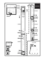
• Refer to page 4-65 for printed wiring board.
4-26
4-27
4-25
I/O SEL, IR, BBI
VC-213 (4/13)
4-28
VC-213
BOARD (4/13)
!£
IC643
!™
CAMERA REC/PB
!¢
IC643
!§
CAMERA REC/PB
1.0Vp-p
H
1.5Vp-p
H
!∞
IC643
@¶
PB
H
0.5Vp-p
H
H
0.3Vp-p
!§
IC643
@ª
PB
!™
IC643
9
, IC644
$¡
CAMERA REC/PB
IR ON
0.5Vp-p
H
!¶
IC643
#¡
PB
0.5Vp-p
!¡
IC643
7
CAMERA REC/PB
2Vp-p
H
Summary of Contents for Digital8 DCR-TRV410
Page 12: ...1 2 ...
Page 13: ...1 3 ...
Page 14: ...1 4 ...
Page 15: ...1 5 ...
Page 16: ...1 6 ...
Page 17: ...1 7 ...
Page 18: ...1 8 ...
Page 19: ...1 9 ...
Page 20: ...1 10 ...
Page 21: ...1 11 ...
Page 22: ...1 12 ...
Page 23: ...1 13 ...
Page 24: ...1 14 ...
Page 25: ...1 15 ...
Page 26: ...1 16 ...
Page 27: ...1 17 ...
Page 28: ...1 18 ...
Page 29: ...1 19 ...
Page 30: ...1 20 ...
Page 31: ...1 21 ...
Page 32: ...1 22 ...
Page 33: ...1 23 ...
Page 34: ...1 24 ...
Page 35: ...1 25 ...
Page 36: ...1 26 ...
Page 37: ...1 27 ...
Page 38: ...1 28 ...
Page 39: ...1 29 ...
Page 40: ...1 30 ...
Page 41: ...1 31 ...
Page 42: ...1 32 ...
Page 43: ...1 33E ...
Page 56: ...DCR TRV410 TRV410E TRV510 TRV510E 3 2 OVERALL BLOCK DIAGRAM 2 3 4 3 5 3 6 ...
Page 58: ...DCR TRV410 TRV410E TRV510 TRV510E 3 10 3 11 3 12E 3 4 POWER BLOCK DIAGRAM 2 ...
Page 79: ...DCR TRV410 TRV410E TRV510 TRV510E 4 73 4 74 STEADY SHOT SE 88 AV IN OUT PJ 97 ...
Page 83: ...DCR TRV410 TRV410E TRV510 TRV510E 4 83 4 84 4 85 USER CONTROL CF 64 ...