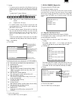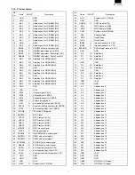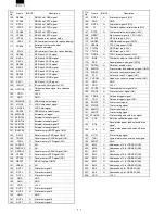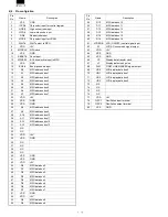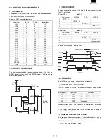
1) CPU INTERFACE
The figure below shows a typical pseudo SRAM interface in the UP-
600.
2) SRAM ADDRESS
Standard SRAM is decoded as follows by the RASPN1 signal.
780000h
∼
7FFFFFh
The base signal is 2MB. It thus wraparounds with 600000H
∼
7FFFFFH 1.5MB.
7. NOR-type FLASH MEMORY
Here is the explanation for the interface of NOR-type flash memory.
The device is Sharp’s LH28F016SU flash memory which consists of
512 K words
×
16 or 1 MB
×
8, with 32 blocks of 64 KB.
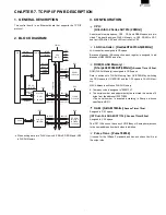
1) CPU INTERFACE
The figure below shows a typical interface for the LH28F016SU of the
UP-600 system.
2) DEVICE CONTROL
After resetting, the device automatically enters the array read mode
and performs the same action as the usual ROM, thus requiring no
special consideration when reading data.
Data can be written at a high speed by using the page buffer.
8. SSP CONTROL
The UP-600 uses flash memory in the place of EPROM, so it is
possible to rewrite the contents of the flash memory in changing the
program. However, since the existing gate array MPCA8 is used, it is
also possible to use the conventional SSP.
1) OPERATION
Like the MPCA5 ~ 8, the MPCA9 adopts the break address register
comparison method for detecting addresses. The operation of this
method is briefly explained below.
The gate array always compares the break address register (BAR)
built in the gate array, with the address bus to monitor the address
bus.
If both agree, the gate array outputs the NMI signal to the CPU, which
in turn shifts from normal handling to exception handling.
In both the MPCA5 ~ 8 and the MPCA9, SSP is achieved by the
above operation.
The setting of the break address register (BAR) is directly written in
the addresses from FFFF00h to FFFFFFh.
9. INTERRUPT CONTROL
There are roughly two types of interrupts:
•
Internal interrupts: Controlled inside the CPU
•
External interrupts: Input into the CPU from outside
1) INTERNAL INTERRUPTS
Device interrupts built in the CPU are used for the following applica-
tions:
Event factor
Application
SC11
Interrupt source as RS232 : CH8
SC12
Not used (SC1 is used for CKDC interface.)
FRT1
(ICI)
(OCRA)
(OCRB)
(OVF)
INTMCR
∼
MCR interrupt (to FT11 terminal)
FRT2
(ICI)
Standard SHEN event (for CKDC)
(OCRA)
Simple IRC timer event
(OCRB)
RS232 timer event
(OVF)
System timer (53 ms)
TMR
(CMA)
(CMB)
(OVF)
WDT
(OVF)
Drawer open timer
A/D
Not used
NMI
SSP request
2) EXTERNAL INTERRUPTS
The following types of external interrupts are available:
•
NMI (SSP)
•
IRQ0 (Standard I/O interrupt)
•
IRQ1 (RS232 interrupt)
•
IRQ2 (Not Used)
•
IRQ3 (Used as SCK terminal)
S RAM(Standard)
A0~A18
A0~A18
A0~A21
D0~D7
D8~D15
/RD
/RD
MPCA9
/WR
/HWR
/CE
S RAM(Option)
A0~
A18
RASPN2
74LV138
A19~
A21
A,B,C
Y
/G
/RESET
RASPN1
RESET-
5V
FVPON
NORDY
H8/510
DATA
RD-
PORT64
PORT63
MPCA8
FROS1-
WE#
OE#
CE0#
GND
VPP
CE1#
RP#
3/5#
VCC
BYTE#
RY/BY#
A0~A2
DQ0~DQ1
WP#
LH28F
016SUT
ADDRES
HWR-
Summary of Contents for UP-600
Page 8: ......
Page 77: ...CHAPTER 9 PWB LAYOUT 1 MAIN PWB 1 A side R VRD RC2EY103J is added IC1 94pin R71 ...
Page 78: ...2 B side Symbol PartsCod ...
Page 79: ...2 CKDC PWB 3 DISPLY MCR PWB 1 A side 2 B side 4 RS232 RELAY PWB 1 A side 2 B side ...
Page 80: ...5 IPL ROM PWB 1 A side 8 POP UP DISPLY 9 LCD I F PWB 2 B side 6 TCP IP RELAY PWB 7 VR PWB ...

