background image

1-5-1

E5752IB

OPERATING CONTROLS AND FUNCTIONS

12

13 14

15

11

10

AV (TV)

AUDIO OUT

VIDEO OUT

S-VIDEO

VIDEO

DIGITAL

R

L

REAR VIEW

2

4

3

5

1

9

8

7

6

OPERATE

OPEN/CLOSE

PLAY

STOP

SKIP

REW

FWD

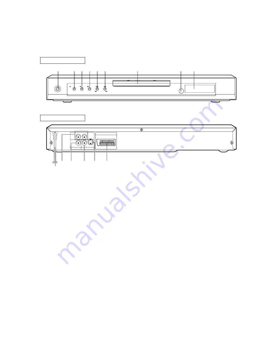
FRONT PANEL

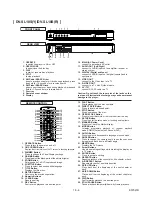
1. OPERATE

to switch the player to ON or OFF

2. OPEN/CLOSE

to open/close the disc tray

3. PLAY

to start or resume disc playback

4. STOP

to stop playback

5. SKIP

H

/ SEARCH

h

goes to previous chapter or track during playback; press
and hold for 1.5 seconds for a reverse search

6. SKIP

G

/ SEARCH 

g

goes to next chapter or track during playback; press and
hold for 1.5 seconds for a forward search

7. Disc tray
8. Remote sensor window
9. Display

10. MAIN (AC Power Cord)

connect to a standard AC outlet

11. AUDIO OUT (Left/Right)

connect to AUDIO inputs of an amplifier, receiver or
stereo system

12. DIGITAL (Digital audio out)

connect to AUDIO inputs of a digital (coaxial) audio
equipment

13. VIDEO OUT

connect to the Video Input of a TV 

14. S-VIDEO OUT

connect to a TV with S-Video inputs

15. AV (TV)

connect SCART cable to a TV

Caution: Do not touch the inner pins of the jacks on the
rear 
damage to the player.

panel. Electrostatic discharge may cause permanent

[ DV-SL10H ]

Summary of Contents for DV-SL10H

Page 1: ...FUNCTION DESCRIPTIONS 1 14 1 LEAD IDENTIFICATIONS 1 15 1 EXPLODED VIEWS 1 16 1 MECHANICAL PARTS LIST 1 17 1 ELECTRICAL PARTS LIST 1 18 1 CONTENTS In the interests of user safety Required by safety regula tions in some countries the set should be restored to its original condition and only parts identical to those specified be used MODELS DV SL10H DV SL10S Y DV SL10S R SERVICE MANUAL DVD VIDEO PLAY...

Page 2: ...1 1 1 E5752SP SPECIFICATIONS DV SL10H DV SL10S Y DV SL10S R ...

Page 3: ...am is emitted from the location shown in the figure When checking the laser diode be sure to keep your eyes at least 30cm away from the pickup lens when the diode is turned on Do not look directly at the laser beam Caution Use of controls and adjustments or doing procedures other than those specified herein may result in hazardous radiation exposure Drive Mecha Assembly Laser Beam Radiation Laser ...

Page 4: ...ur être sûr que les fils ne sont pas pincés ou que le matériel n est pas coincé entre le châssis et les autres pièces métalliques dans le reproductor de vídeo DVD 2 Vérifier tous les dispositifs de protection tels que les boutons de commande non métalliques les matériaux d isolement le dos du coffret les couvercles de compartiment et ajustement ou les boucliers les réseaux de résistance condensate...

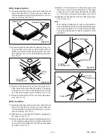
Page 5: ... chine then apply hot air to the Flat Pack IC about 5 to 6 seconds Fig S 1 1 Fig S 1 1 2 Remove the flat pack IC with tweezers while apply ing the hot air 3 Bottom of the flat pack IC is fixed with glue to the CBA when removing entire flat pack IC first apply soldering iron to center of the flat pack IC and heat up Then remove glue will be melted Fig S 1 6 4 Release the flat pack IC from the CBA u...

Page 6: ... remove the solder from all pins of the flat pack IC When you use solder flux which is applied to all pins of the flat pack IC you can remove it easily Fig S 1 3 2 Affix the wire to a workbench or solid mounting point as shown in Fig S 1 5 3 While heating the pins using a fine tip soldering iron or hot air blower pull up the wire as the solder melts so as to lift the IC leads from the CBA contact ...

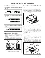
Page 7: ... IC Fig S 1 8 Instructions for Handling Semi conductors Electrostatic breakdown of the semi conductors may occur due to a potential difference caused by electrostatic charge during unpacking or repair work 1 Ground for Human Body Be sure to wear a grounding band 1MΩ that is properly grounded to remove any static electricity that may be charged on the body 2 Ground for Workbench Be sure to place a ...

Page 8: ... SKIP G SEARCH g goes to next chapter or track during playback press and hold for 1 5 seconds for a forward search 7 Disc tray 8 Remote sensor window 9 Display 10 MAIN AC Power Cord connect to a standard AC outlet 11 AUDIO OUT Left Right connect to AUDIO inputs of an amplifier receiver or stereo system 12 DIGITAL Digital audio out connect to AUDIO inputs of a digital coaxial audio equipment 13 VID...

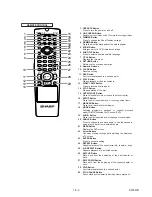
Page 9: ...P Button Press to locate a desired point 14 STOP Button Stops operation of the disc 15 OPEN CLOSE Button Press to insert discs into or remove them from the tray 16 SETUP Button Press to enter the setup mode or to change setup items 17 MARKER Button Press to call back the Marker display 18 MODE Button Activates programme playback or random playback mode CD MP3 Activates the 3D sound DVD 19 AUDIO Bu...

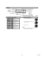
Page 10: ...Stays on when repeat chapter function is on Stays on when repeat track function is on Stays on when the A B repeat function is on Stays on when the repeat function is on Stays on when repeat title function is on Displays how long a current title or track has been played back When a chapter or track has switched the number of a new title chapter or track is displayed CD Lights up when a CD is inser...

Page 11: ... desired point 14 STOP Button Stops operation of the disc 15 OPEN CLOSE Button Press to insert discs into or remove them from the tray 16 SETUP Button Press to enter the setup mode or to change setup items 17 MARKER Button Press to call back the Marker display 18 MODE Button Activates programme playback or random playback mode CD MP3 Activates the 3D sound DVD 19 AUDIO Button Press to select a des...

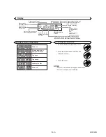
Page 12: ...se Stays on when repeat chapter function is on Stays on when repeat track function is on Stays on when the A B repeat function is on Stays on when the repeat function is on Stays on when repeat title function is on Displays how long a current title or track has been played back When a chapter or track has switched the number of a new title chapter or track is displayed CD Lights up when a CD is in...

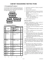
Page 13: ...e and then three Locking Tabs B at the bottom Fig 2 1 7 Release three Locking Tabs L 4 Then remove the Front Assembly CAUTION 2 Electrostatic breakdown of the laser diode in the optical system block may occur as a potential difference caused by electrostatic charge accumulated on cloth human body etc during unpacking or repair work To avoid damage of pickup follow next procedures 2 1 Disconnect Co...

Page 14: ...lands by soldering Short the three short lands by soldering FPC Cable Connector Slide DVD Mecha View for C View for A OR A Fig 1 Fig 2 Fig 3 Fig 4 S 1 S 1 1 Top Cover S 1 2 Front Assembly Tray Panel A A L 3 L 3 L 1 L 1 B L 2 L 4 L 4 3 DVD Mecha S 2 S 2 CN201 CN301 ...

Page 15: ...2 Rotate the roulette in the direction of the arrow as shown below S 7 8 Rear Panel S 6 7 Main CBA Holder Rotate this roulette in the direction of the arrow A View for A Fig 5 4 AV CBA 5 DVD Main CBA S 5 S 3 S 4 CN1601 CN1001 S 4 6 Function CBA Desolder from bottom ...

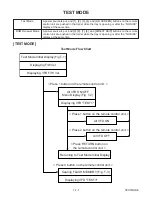
Page 16: ... tray is opening or after the NO DISC display at the same time TEST MODE Test Mode Flow Chart Test Mode Initial Display Fig T 1 Displaying F W Ver Displaying VFD F W Ver Press 1 button on the remote control unit Press 1 button on the remote control unit Press 2 button on the remote control unit Press 3 button on the remote control unit Press RETURN button on the remote control unit Returning to Te...

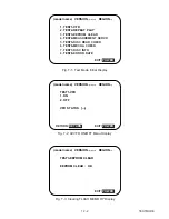
Page 17: ...RSION REGION 1 TEST1 VFD 2 TEST2 REPEAT PLAY 3 TEST3 EEPROM CLEAR 4 TEST4 MEASUREMENT SERVO 5 TEST5 DISC READ CHECK 6 TEST6 MECHA CHECK 7 TEST7 DISC INFO 8 TEST8 ERROR RATE EXIT model name VERSION REGION TEST1 VFD 1 ON 2 OFF VFD STATUS RETURN POWER model name VERSION REGION TEST3 EEPROM CLEAR EEPROM CLEAR OK EXIT POWER EXIT POWER RETURN ...

Page 18: ...escribed as follows Appearance No State Reading Sending files into the memory Erasing Erasing previous version data Programming 1 2 3 Writing new version data 5 After programming is finished the tray opens auto matically Fig e appears on the screen and the checksum in 3 of Fig e appears on the VFD Fig f F W Version Up Mode VERSION Completed SUM 7abc 3 Fig e Completed Program Mode Screen Fig f VFD ...

Page 19: ...hed and error rate measurement will begin Fig c will display 1 Inserted disk s inner parameter For DVD Layer 0 initial address 2 Inserted disk s outer parameter For DVD Layer 0 final address 3 Inserted disk s Layer 1 initial address 4 Inserted disk s Layer 1 final address Depending on the contents of the inserted disk 3 and 4 above may not be displayed Once the error rate measurement has started i...

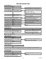
Page 20: ...ltage supplied to the anode of D1003 Check D1003 and periphery circuit and service it if defective Check if there is any leak or short circuit on the loaded circuit and service it if defective Yes No FLOW CHART NO 1 The power cannot be turned on Is the fuse normal Is normal state restored when once unplugged power cord is plugged again after several seconds Is each voltage of the secondary side no...

Page 21: ...8 L1009 C1035 C1048 and the periphery circuit and service it if defective Check Q1016 and PWRCON line and service it if defective Yes Yes No No FLOW CHART NO 7 EV 9V is not outputted Is 9V voltage supplied to the collector of Q1050 Is the H pulse inputted into the base of Q1050 Replace Q1050 Check D1030 D1048 L1009 C1035 C1048 R1097 and the periphery circuit and service it if defective Check D1072...

Page 22: ...f defective Check or replace the power circuit D1016 D1017 T1001 and their periphery and service it if defective Is the voltage of 17V supplied to the collector of Q1005 FLOW CHART NO 14 The key operation is disabled Is key switch contact SW2001 SW2003 2005 2006 2008 and installation state normal Is the control voltage normally inputted into Pins 7 8 of IC2002 Check the key switches SW2001 SW2003 ...

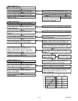
Page 23: ...plied to the Pin 20 of IC2002 when the infrared remote control is activated Yes Yes Yes Is 5V voltage supplied to the Pin 3 terminal of the infrared remote control receiver Yes No No Check EV 5V line and service it if defective No No FLOW CHART NO 16 The disc tray cannot be opened and closed It can be done using the remote control unit Is 0 49V to 1 49V voltage inputted into Pin 8 of IC2002 when t...

Page 24: ...Main CBA is poor FLOW CHART NO 19 No Disc indicated When the focus servo is not functioning FLOW CHART NO 20 No Disc indicated When the laser beam does not light up Replace the DVD Main CBA Replace the DVD Mecha No Yes Replace the DVD Main CBA Replace the DVD Mecha No Yes No improvement can be found Original DVD Main CBA is poor No improvement can be found Original DVD Main CBA is poor ...

Page 25: ...Y CN1601 9PIN S C CN1601 7PIN G CN1601 5PIN B CN1601 3PIN R IC1402 6PIN S Y IC1402 2PIN S C IC1402 16PIN G IC1402 12PIN B IC1402 14PIN R IC1402 31PIN CVBS IC1402 28PIN S Y IC1402 33PIN S C IC1402 19PIN G IC1402 25PIN B IC1402 22PIN R Check the periphery of JK1404 from Pins 19 22 25 of IC1401 and service it if detective Check the periphery of JK1402 and JK1404 from Pin 31 of IC1401 and service it i...

Page 26: ...ce the DVD Main CBA or DVD Mecha Replace the DVD Main CBA or DVD Mecha Replace IC1201 Check the periphery between Pins 1 7 of IC1201 and JK1402 and service it if detective Check each line between each pin of CN1601 and each pin of IC1201 on AV CBA and service it if detective CN1601 13PIN IC1201 2PIN AUDIO L CN1601 15PIN IC1201 6PIN AUDIO R Are the analog audio signals inputted to each pin of IC120...

Page 27: ...TO DIGITAL SIGNAL PROCESS BLOCK DIAGRAM FS FS TS TS TO VIDEO AUDIO BLOCK DIAGRAM 51 ADAC MD 50 ADAC MC 96 ADAC ML ADAC MC ADAC ML PCM SCLK 95 A MUTE ADAC MD A MUTE 17 92 FSEL RESET 68 RESET IC461 5 4 3 3V TRAY OUT TRAY IN FOCUS SERVO SIGNAL TRACKING SERVO SIGNAL SLED SERVO SIGNAL SPINDLE SERVO SIGNAL 3 SP 4 SP 5 TRAY OUT 6 TRAY IN 7 GND 8 SL 9 SL 1 FG IN 64 ASPECT ASPECT 63 PWRCON CN1001 2 28 27 1...

Page 28: ...WATCH DOG TIMER 32BIT CPU STREAM I F EXTERNAL MEMORY I F SDRAM ECC UMAC 124 125 122 123 128 129 126 127 131 130 135 133 132 134 78 DEBUG BCU INST CACHE D TYPE LATCH DATA CACHE D A D A D A TO VIDEO AUDIO BLOCK DIAGRAM 158 164 G C R B VIDEO G VIDEO C VIDEO R VIDEO B TO VIDEO AUDIO BLOCK DIAGRAM 181 SPDIF 175 PCM BCK 176 PCM DATA0 174 PCM LRCLK 161 160 EXADT 0 15 EXADR 16 19 EXADT 0 15 EXADR 16 19 EX...

Page 29: ...AC MC ADAC ML PCM SCLK AV CBA DVD MAIN CBA UNIT AUDIO SIGNAL DATA AUDIO SIGNAL 18 18 SPDIF A MUTE 3 3V Q1204 WF6 3 WF4 WF5 CN601 VIDEO Y VIDEO C FROM DIGITAL SIGNAL PROCESS BLOCK DIAGRAM VIDEO SIGNAL 5V JK1404 1 3 AUDIO L OUT AUDIO R OUT FIBER OPTIC TRANS MODULE IC1204 JK1401 S VIDEO OUT COMPOSITE VIDEO OUT CN1601 1 1 VIDEO Y 9 9 VIDEO C 3 4 2 1 IC1401 VIDEO DRIVER 6 28 4dB AMP 2dB AMP LPF DRIVER ...

Page 30: ...04 FL EV 5V F2 F1 P ON 12V EV 3 3V P ON 5V P ON 3 3V FROM TO CN401 1 2 3 EV 1 5V 4 5 EV 3 3V 14 15 EV 9V 13 P ON 5V 17 P ON 3 3V 1 5V REG IC1002 CAUTION Fixed voltage or Auto voltage selectable power supply circuit is used in this unit If Main Fuse F1001 is blown check to see that all components in the power supply circuit are not defective before you connect the AC plug to the AC power supply Oth...

Page 31: ... 70 C SR Z Capacitors and transistors are represented by the following symbols SCHEMATIC DIAGRAMS CBA S AND TEST POINTS Notes 1 Do not use the part number shown on these draw ings for ordering The correct part number is shown in the parts list and may be slightly different or amended since these drawings were prepared 2 All resistance values are indicated in ohms K 103 M 106 3 Resistor wattages ar...

Page 32: ...on and reliability of repaired units use only original replacement parts which are listed with their part numbers in the parts list section of the service manual 4 Wire Connectors 1 Prefix symbol CN means connector can disconnect and reconnect 2 Prefix symbol CL means wire solder holes of the PCB wire is soldered directly 5 Voltage indications for PLAY modes on the schematics are as shown below 2 ...

Page 33: ...DVD Main 1 3 Schematic Diagram 1 10 3 1 10 4 E5752SCD1 ...

Page 34: ...DVD Main 2 3 Schematic Diagram 1 10 5 1 10 6 E5752SCD2 ...

Page 35: ... 0 2 0 32 64 0 8 0 8 96 3 4 3 4 128 2 0 2 0 PIN NO PLAY STOP PIN NO PLAY STOP PIN NO PLAY STOP PIN NO PLAY STOP 129 2 0 2 0 161 0 5 0 5 193 225 1 9 1 9 130 2 2 2 2 162 1 4 1 4 194 0 0 226 3 3 3 3 131 2 3 2 3 163 0 5 0 5 195 3 3 3 3 227 132 0 4 0 1 164 0 9 0 9 196 228 133 1 2 0 4 165 3 3 3 3 197 229 134 0 4 0 1 166 1 5 1 5 198 0 0 230 0 0 135 0 2 0 2 167 0 0 199 231 136 2 3 2 3 168 2 1 2 1 200 232 ...

Page 36: ...DVD Main 3 3 Schematic Diagram 1 10 9 1 10 10 E5752SCD3 Note IC103 is not supplied separately Be sure to replace with the DVD Main CBA unit when servicing IC103 ...

Page 37: ... selectable power supply circuit is used in this unit If Main Fuse F1001 is blown check to see that all components in the power supply circuit are not defective before you connect the AC plug to the AC power supply Otherwise it may cause some components in the power supply circuit to fail CAUTION FOR CONTINUED PROTECTION AGAINST FIRE HAZARD REPLACE ONLY WITH THE SAME TYPE FUSE ...

Page 38: ...AV 2 3 Schematic Diagram 1 10 13 1 10 14 E5752SCAV2 ...

Page 39: ...f 1 3 2 4 5 DVD VCD PBC STANDBY A B REPEAT TRK CHP TITLE 7G 6G 5G 4G 3G 2G 1G a b c d e f g c d e f g c d e f g c d e f g c d e f g c d e f g h i a b a b a b a b a b FL2001 MATRIX CHART STANDBY TITLE CHP TRK CD V PBC DVD REPEAT A B 1 3 2 4 5 1 10 15 1 10 16 E5752SCAV3 ...

Page 40: ...1 10 17 1 10 18 DVD Main CBA Top View BE5700G04012 ...

Page 41: ...1 10 19 1 10 20 DVD Main CBA Bottom View BE5700G04012 ...

Page 42: ...lectable power supply circuit is used in this unit If Main Fuse F1001 is blown check to see that all components in the power supply circuit are not defective before you connect the AC plug to the AC power supply Otherwise it may cause some components in the power supply circuit to fail CAUTION FOR CONTINUED PROTECTION AGAINST FIRE HAZARD REPLACE ONLY WITH THE SAME TYPE FUSE ...

Page 43: ...D as a common terminal CAUTION Fixed voltage or Auto voltage selectable power supply circuit is used in this unit If Main Fuse F1001 is blown check to see that all components in the power supply circuit are not defective before you connect the AC plug to the AC power supply Otherwise it may cause some components in the power supply circuit to fail CAUTION FOR CONTINUED PROTECTION AGAINST FIRE HAZA...

Page 44: ...Function CBA Top View Function CBA Bottom View BE5714F01014 1 10 25 1 10 26 ...

Page 45: ...STOP MODE WF1 WF3 WAVEFORMS WF6 SPDIF Pin 18 of CN1601 1V 0 1µsec WF1 Pin 1 of CN1601 WF3 Pin 31 of IC1401 WF4 AUDIO L Pin 13 of CN1601 1V 0 5msec WF5 AUDIO R Pin 15 of CN1601 1V 0 5msec WF2 Pin 9 of CN1601 VIDEO Y 0 2V 20µsec VIDEO C 0 2V 20µsec VIDEO CVBS 0 5V 20µsec ...

Page 46: ...001 VIDEO R 3 3 GND 4 4 VIDEO Y 1 1 ASPECT 2 2 VIDEO B 5 5 A MUTE 12 12 GND 11 11 GND 6 6 VIDEO G 7 7 GND 8 8 VIDEO C 9 9 GND 10 10 CN601 CN1601 AC CORD AUDIO L OUT AUDIO R OUT VIDEO OUT DIGITAL AUDIO OUT S VIDEO OUT EV 1 5V 3 3 DRIVE CBA 19 20 SPDIF 18 18 AUDIO L 13 13 A L MUTE 14 14 AUDIO R 15 15 A R MUTE 16 16 AUDIO 5V 17 17 GND VREF P ON 5V F E C B D A PD MONI DVD LD GND LD GND DVD PD TS FS FS...

Page 47: ...lose Play Play Tray Open Tray IN TL221 3 3V 0V 0V 3 3V 0V 1 65V 0V 0V 0V 1 65V 1 65V 1 65V Tray OUT TL220 Sled Drive TP303 Disc Drive TP301 Focus Drive TP304 Tracking Drive Tracking Drive TP302 TP302 Tray Close Disc Rotation Play Disc Stop Tray Open ...

Page 48: ... Out 7G Grid Output 18 6G 19 5G 20 4G 21 3G 22 2G 23 1G 24 VDD Power Supply 25 VSS GND 26 In OSC Oscillator Input 27 Out DOUT Serial Data Output 28 In DIN Serial Data Input IC2002 M34506M4 504FP Pin No In Out Signal Name Name Function 1 VDD Power supply 2 Vss GND 3 In Xin Sub Clock Input 4 Out Xout Sub Clock Output 5 CNVSS CNVSS 6 In Out RESET Reset Input Output Signal 7 In K1 Key Data 1 Input Sig...

Page 49: ...C2120 Y TPE2 KTC3205 Y 2SC2236 Y TPE6 C 2SA966 Y E C B 2SC2785 H KTC3199 GR KRA110M KTA1267 Y BN1L3Z P A K C E LTV 817 B C F KIA431 AT G D S 2SK3566 PQ070XF01SZ K A R 1 2 3 4 Note A Anode K Cathode E Emitter C Collector B Base R Reference G Gate D Drain S Source 1 Vin 2 Vo 3 GND 4 Vc 34 18 17 MM1567AJ 1 20 11 10 1 M34506M4 504FP ...

Page 50: ...05 W1601 W1001 2L031 2L021 A2 2L021 2L021 A13 2L011 2L011 2L011 A16 2L011 2L011 2L041 A13 A1X 2L101 AC1001 A21 DVD Main CBA Unit See Electrical Parts List for parts with this mark Some Ref Numbers are not in sequence AV CBA 1B1 FUNCTION CBA F1001 JK1402 JK1404 JK1401 W2101 ...

Page 51: ...1 16 2 E5752EX Packing X10 X2 X4 S2 S2 S4 Unit S1 S5 X1 X17 DV SL10H only A22 A30 ...

Page 52: ...ABEL E57B3ED AB A30 C CASE MARK LABEL E57B4ED AB 1B1 DVD MECHA THIN TYPE 0838 VCDVM040 9HSN79F1GVM BS 2B3 HOLDER MAIN PCB E5700UD 9HS0VM305832B AC 2L011 SCREW C TIGHT M3X5 BIND HEAD 9HSGBCC3050 AA 2L021 SCREW S TIGHT M3X8 BIND CHROME 9HSGBMS3080 AA 2L031 SCREW C TIGHT M3X6 BIND HEAD 9HSGBMC3060 AA 2L041 SCREW B TIGHT M3X8 BIND HEAD 9HSGBKB3080 AA 2L071 SCREW C TIGHT M3X6 BIND HEAD 9HSGBMC3060 AA 2...

Page 53: ... F Z 0 1µF 16V 9HSHB1CZ30F104 AA C113 CHIP CERAMIC CAP 1005 F Z 0 1µF 16V 9HSHB1CZ30F104 AA C114 CHIP CERAMIC CAP 1005 F Z 0 1µF 16V 9HSHB1CZ30F104 AA C116 CHIP CERAMIC CAP 1005 F Z 0 1µF 16V 9HSHB1CZ30F104 AA C117 CHIP CERAMIC CAP 1005 F Z 0 1µF 16V 9HSHB1CZ30F104 AA C118 CHIP CERAMIC CAP 1005 F Z 0 1µF 16V 9HSHB1CZ30F104 AA C119 CHIP CERAMIC CAP 1005 F Z 0 1µF 16V 9HSHB1CZ30F104 AA C120 CHIP CER...

Page 54: ...V 9HSHB1AK30B104 AA C284 CHIP CERAMIC CAP 1005 B K 0 01µF 25V 9HSHB1EK30B103 AA C301 CHIP CERAMIC CAP 1005 B K 0 1µF 10V 9HSHB1AK30B104 AA C303 CHIP CERAMIC CAP 1005 CH J 180pF 50V 9HSHB1JJ3CH181 AA C305 CHIP CERAMIC CAP 1005 B K 6800pF 25V 9HSHB1EK30B682 AA C306 CHIP CERAMIC CAP 1005 B K 6800pF 25V 9HSHB1EK30B682 AA C308 CHIP CERAMIC CAP 1005 B K 0 01µF 25V 9HSHB1EK30B103 AA C309 CHIP ELECTROLYTI...

Page 55: ...16V 9HSHB1CZ30F104 AA C656 CHIP ELECTROLYTIC CAP 47µF 6 3V WX WR 9HSA0K470NC156 AC C656 CHIP ELECTROLYTIC CAP 47µF 6 3V M BSS 9HSA0K470SP057 AC C657 CHIP ELECTROLYTIC CAP 330µF 6 3V UR 9HSE0KMR1FL331 AD C657 CHIP ELECTROLYTIC CAP 330µF 6 3V M 9HSA0K331SP012 AD C658 CHIP ELECTROLYTIC CAP 330µF 6 3V UR 9HSE0KMR1FL331 AD C658 CHIP ELECTROLYTIC CAP 330µF 6 3V M 9HSA0K331SP012 AD CONNECTORS CN201 FFC F...

Page 56: ...S 100PPM 1 16W F 15k Ω 9HSRXGFR5H1502 AA R113 CHIP RES 1608 1 10W F 27k Ω 9HSRXAFR5H2702 AA R113 CHIP RES 100PPM 1 16W F 27k Ω 9HSRXGFR5H2702 AA R114 CHIP RES 1608 1 10W F 18k Ω 9HSRXAFR5H1802 AA R114 CHIP RES 100PPM 1 16W F 18k Ω 9HSRXGFR5H1802 AA R116 CHIP RES 1608 1 10W F 15k Ω 9HSRXAFR5H1502 AA R116 CHIP RES 100PPM 1 16W F 15k Ω 9HSRXGFR5H1502 AA R117 CHIP BEAD MMZ1608Y121BT 9HSL06001TE006 AB ...

Page 57: ...XAZR5Z0000 AA R334 CHIP RES 1608 1 10W 0 Ω 9HSRXAZR5Z0000 AA R422 CHIP RES 1608 1 10W J 4 7k Ω 9HSRXAJR5Z0472 AA R451 CHIP BEAD MMZ1608Y121CT 9HSL06001TE004 AB R453 CHIP INDUCTOR BK1608HM471 T 9HSLBC003TU053 AB R454 CHIP RES 1608 1 10W 0 Ω 9HSRXAZR5Z0000 AA R456 CHIP RES 1608 1 10W J 47 Ω 9HSRXAJR5Z0470 AA R457 CHIP RES 1608 1 10W J 240 Ω 9HSRXAJR5Z0241 AA R459 CHIP RES 1608 1 10W 0 Ω 9HSRXAZR5Z00...

Page 58: ... C1004 ELECTROLYTIC CAP 33µF 400V M 105C 9HSA2H330NC162 AG C1005 CERAMIC CAP SL K 56pF 1KV 9HSCD3AKPSL560 AC C1006 SAFETY CAP 2200pF 250V 9HSCN2EMP0E222 AD C1006 SAFETY CAP 2200pF 250V 9HSA2E222MR049 AD C1007 ELECTROLYTIC CAP 1000µF 6 3V M 9HSE0KMASDL102 AC C1009 ELECTROLYTIC CAP 2200µF 6 3V M 9HSE0KMASTL222 AC C1010 CERAMIC CAP AX CH J 560pF 50V 9HSA1J561TU008 AA C1013 CERAMIC CAP AX B K 3300pF 5...

Page 59: ...YTIC CAP 470µF 6 3V M 9HSE0KMASDL471 AB C1486 ELECTROLYTIC CAP 1µF 50V M 9HSE1JMASDL010 AB C1487 CHIP CERAMIC CAP CH J 1000pF 50V 9HSHD1JJ3CH102 AA C1491 ELECTROLYTIC CAP 1µF 50V M 9HSE1JMASDL010 AB C1492 ELECTROLYTIC CAP 470µF 6 3V M 9HSE0KMASDL471 AB C1521 CHIP CERAMIC CAP CH J 100pF 50V 9HSHD1JJ3CH101 AA C1522 ELECTROLYTIC CAP 10µF 16V M 9HSE1CMASDL100 AB C1523 CHIP CERAMIC CAP CH J 100pF 50V 9...

Page 60: ...M 9HSDTZ01N4148M AA D1055 SWITCHING DIODE 1SS133 T 77 9HSDTZ001SS133 AB D1056 SWITCHING DIODE 1N4148M 9HSDTZ01N4148M AA D1056 SWITCHING DIODE 1SS133 T 77 9HSDTZ001SS133 AB D1058 RECTIFIER DIODE 1N4005 9HSDQZ001N4005 AB D1072 ZENER DIODE DZ 10BSBT265 9HSDTB00DZ10BS AB D1072 ZENER DIODE MTZJT 7710B 9HSDTB00MTZJ10 AB D1074 RECTIFIER DIODE 1N4005 9HSDQZ001N4005 AB D1075 RECTIFIER DIODE 1N4005 9HSDQZ00...

Page 61: ...S Q1001 FET 2SK3566 9HSFWZ02SK3566 AH Q1002 TRANSISTOR KTA1267 Y 9HSQSY0KTA1267 AC Q1003 TRANSISTOR KTC3199 GR 9HSQS10KTC3199 AB Q1003 TRANSISTOR 2SC2785 H 9HSQSH02SC2785 AB Q1004 TRANSISTOR KTC3198 Y 9HSQSY0KTC3198 AB Q1005 TRANSISTOR KTC3198 Y 9HSQSY0KTC3198 AB Q1006 RES BUILT IN TRANSISTOR KRA110M 9HSQSZ0KRA110M AB Q1006 RES BUILT IN TRANSISTOR BN1L3Z P 9HSQSP00BN1L3Z AC Q1008 TRANSISTOR KTC319...

Page 62: ...X4JATZ0473 AA R1037 CARBON RES 1 4W J 10k Ω 9HSCX4JATZ0103 AA R1038 CARBON RES 1 6W J 100k Ω 9HSCX6JATZ0104 AA R1038 CARBON RES 1 4W J 100k Ω 9HSCX4JATZ0104 AA R1039 CARBON RES 1 4W J 470k Ω 9HSCX4JATZ0474 AA R1043 METAL OXIDE FILM RES 1W J 2 7 Ω 9HSN012R7ZU001 AA R1043 METAL OXIDE FILM RES 1W J 2 7 Ω 9HSN012R7KE009 AA R1044 CHIP RES 1608 1 10W J 100k Ω 9HSRXAJR5Z0104 AA R1059 CHIP RES 1608 1 10W ...

Page 63: ...608 1 10W J 100k Ω 9HSRXAJR5Z0104 AA R1392 CHIP RES 1608 1 10W J 1k Ω 9HSRXAJR5Z0102 AA R1396 CHIP RES 1608 1 10W J 1k Ω 9HSRXAJR5Z0102 AA R1397 CHIP RES 1608 1 10W J 100 Ω 9HSRXAJR5Z0101 AA R1402 CHIP RES 1608 1 10W J 75 Ω 9HSRXAJR5Z0750 AA R1405 CARBON RES 1 6W J 75 Ω 9HSCX6JATZ0750 AA R1405 CARBON RES 1 4W J 75 Ω 9HSCX4JATZ0750 AA R1421 CHIP RES 1 16W F 75 Ω 9HSRXGFR5Z0750 AA R1422 CHIP RES 160...

Page 64: ...AJ 2050 040 9HSXGL210JD002 AG RM2001 REMOTE RECEIVER PIC 37043LU 9HSSESJRSKK039 AR SA1001 SURGE ABSORBER PVR 10D471KB 9HSVQZ10D471KB AC SA1001 SURGE ABSORBER CNR 10D471K 9HSVQZR10D471K AC SW2001 TACT SWITCH KSM0614B 9HSST0101HH013 AB SW2001 TACT SWITCH SKQSAF001A 9HSST0101AL041 AA T1001 POWER TRANSFORMER CSA SW0215C 9HSTT00EPSA141 AH W1001 22P FFC AV PCB TO MAIN 9HSX1E57S0 002 AG W1601 18P FFC 9HS...

Page 65: ...PYRIGHT 2003 BY SHARP CORPORATION ALL RIGHTS RESERVED No part of this publication may be reproduced stored in a retrieval system or transmitted in any form or by any means electronic mechanical photocopying recording or otherwise without prior written permission of the publisher Jun 2003 Printed in JAPAN ...

Reviews: