1-8-2
E5752TS
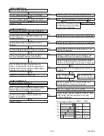
FLOW CHART NO.8
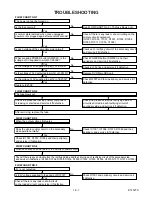
P-ON+5V is not outputted. (EV+9V is outputted normally.)
Is the "H" pulse inputted into the base of Q1004?
Replace Q1004.
Check R1068 and D1046, and service it if defective.
Yes
No
FLOW CHART NO.9
P-ON+3.3V is not outputted. (P-ON+12V is outputted normally.)
Is 3.3V voltage supplied to the collector of Q1011?
Replace Q1011 and R1067.
Check D1008, D1015, C1007, C1038 and the
periphery circuit, and service it if defective.
Yes
No
FLOW CHART NO.11
EV+5V is not outputted.
Is EV+9V outputted normally?
Refer to "FLOW CHART NO.7"
<EV+9V is not outputted.>
Yes
No
Replace Q1014.
FLOW CHART NO.6
P-ON+12V is not outputted.
Is 12V voltage supplied to the emitter of Q1002?
Is the voltage of base on Q1002 lower than the
voltage of emitter on Q1002 when turning the power on?
Replace Q1002.
Check D1030, D1048, L1009, C1035, C1048 and
the periphery circuit, and service it if defective.
Check Q1016 and PWRCON line and service it if
defective.
Yes
Yes
No
No
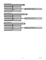
FLOW CHART NO.7
EV+9V is not outputted.
Is 9V voltage supplied to the collector of Q1050?
Is the "H" pulse inputted into the base of Q1050?
Replace Q1050.
Check D1030, D1048, L1009, C1035, C1048, R1097
and the periphery circuit, and service it if defective.
Check D1072, C1070, R1098 and service it if
defective.
Yes
Yes
No
No
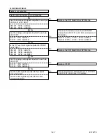
FLOW CHART NO.10
EV+3.3V is not outputted.
Is 3.3V voltage supplied to the emitter of Q1010?
Is the "L" pulse inputted into the base of Q1012?
Is the "H" pulse inputted into the base of Q1014?
Yes
Replace IC2002.
Check the circuit between
Pin(19) of IC2002 and Q1012,
and service it if defective.
Check D1008, D1015, C1007, C1038 and the
periphery circuit, and service it if defective.
Check Q1012, Q1010, R1087 and R1088,
and service it if defective.
Is the "L" pulse outputted to Pin(19) of IC2002?
Yes
Yes
Yes
No
No
No
Check D1047, R1069, and service it if defective.
No
Summary of Contents for DV-SL10H
Page 2: ...1 1 1 E5752SP SPECIFICATIONS DV SL10H DV SL10S Y DV SL10S R ...
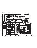
Page 33: ...DVD Main 1 3 Schematic Diagram 1 10 3 1 10 4 E5752SCD1 ...
Page 34: ...DVD Main 2 3 Schematic Diagram 1 10 5 1 10 6 E5752SCD2 ...
Page 38: ...AV 2 3 Schematic Diagram 1 10 13 1 10 14 E5752SCAV2 ...
Page 40: ...1 10 17 1 10 18 DVD Main CBA Top View BE5700G04012 ...
Page 41: ...1 10 19 1 10 20 DVD Main CBA Bottom View BE5700G04012 ...
Page 44: ...Function CBA Top View Function CBA Bottom View BE5714F01014 1 10 25 1 10 26 ...
Page 51: ...1 16 2 E5752EX Packing X10 X2 X4 S2 S2 S4 Unit S1 S5 X1 X17 DV SL10H only A22 A30 ...


