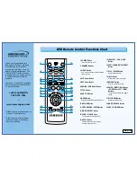
1-10-3
H9740TS
Yes
Yes
Yes
Yes
No
No
No
No
FLOW CHART NO.14
DVD-P-ON+12V is not outputted. (AL+12V is outputted normally.)
FLOW CHART NO.11
Replace Q1053.
No
Yes
Is the "L" pulse (approximately 0V) outputted to
the collector of Q1054?
Check Q1054 and PWRCON line, and service it if
defective.
FLOW CHART NO.13
DVD-P-ON+3.3V is not outputted. (EV+3.3V is outputted normally.)
Is the "H" pulse (approximately 4V) inputted to
the base of Q1052?
Replace Q1052.
See FLOW CHART NO.11. <DVD-P-ON+12V is
not outputted. >
Yes
No
FLOW CHART NO.12
DVD-P-ON+5V is not outputted. (AL+5V is outputted normally.)
Is the "H" pulse (approximately 6V) inputted to
the base of Q1055?
Replace Q1055.
See FLOW CHART NO.11. <DVD-P-ON+12V is
not outputted. >
Yes
No
The fluorescent display tube does not light up.
Is 3.3V voltage supplied to Pin(6, 24) of IC612?
Is approximately -24V to -28V voltage supplied to
Pin(15) of IC612?
Is there approximately 500kHz oscillation to
Pin(26) of IC612?
Are the filament voltage applied between (1, 2)
and (29, 30) of the fluorescent display tube?
Also negative voltage applied between these pins
and GND?
Replace the fluorescent display tube (IC611).
Check the EV+3.3V line and service it if defective.
Check the -FL line and service it if defective.
Check R618, IC612 and their periphery, and
service it if defective.
Check the power circuit, D1016, D1017,
R1040, C1018 and their periphery, and
service it if defective.
Summary of Contents for DV-NC100S
Page 48: ...1 12 3 1 12 4 H9740SCM1 Main 1 9 Schematic Diagram VCR Section ...
Page 50: ...Main 3 9 Schematic Diagram VCR Section 1 12 7 1 12 8 H9740SCM3 ...
Page 51: ...Main 4 9 Schematic Diagram VCR Section 1 12 9 1 12 10 H9740SCM4 ...
Page 52: ...1 12 11 1 12 12 H9740SCM5 Main 5 9 Schematic Diagram VCR Section ...
Page 53: ...Main 6 9 Schematic Diagram VCR Section 1 12 13 1 12 14 H9740SCM6 ...
Page 54: ...Main 7 9 DVD Open Close Schematic Diagrams VCR Section 1 12 15 1 12 16 H9740SCM7 ...
Page 55: ...Main 8 9 Schematic Diagram VCR Section 1 12 17 1 12 18 H9740SCM8 ...
Page 56: ...1 12 19 1 12 20 H9740SCM9 Main 9 9 Schematic Diagram VCR Section ...
Page 58: ...Jack A Schematic Diagram 1 12 23 1 12 24 H9740SCJ ...
Page 59: ...AFV Schematic Diagram 1 12 25 1 12 26 H9740SCAFV ...
Page 60: ...1 12 27 1 12 28 H9740SCD1 DVD Main 1 3 Schematic Diagram DVD Section ...
Page 61: ...1 12 29 1 12 30 H9740SCD2 DVD Main 2 3 Schematic Diagram DVD Section ...
Page 69: ...1 12 46 BE5900G04012 1 12 45 DVD MAIN CBA Top View ...
Page 70: ...1 12 47 1 12 48 BE5900G04012 DVD MAIN CBA Bottom View ...