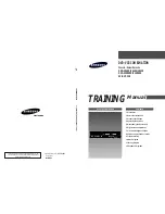


DVD-VCR COMBINATION
Chassis : Diva
SV-DVD50
TRAINING
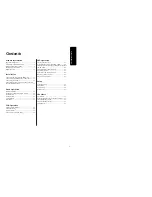
1. Precautions
2. Reference Information
3. Product Specification
4. Operating Instructions
5. Disassembly and Reassembly
6. Alignment and Adjustment
7. Circuit Operating Description
8. VCR Deck Operating Description
9. Troubleshooting
10. Block Diagram
11. Wiring Diagram
12. Schematic Diagrams
Manual
DVD-VCR COMBINATION
CONTENTS
TRAINING MANUAL
SV
-DVD50
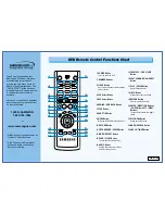
EJECT
STANDBY/ON
DVD
PROG
VCR
AUX
ELECTRONICS
© Samsung Electronics Co., Ltd.
MAR. 2003
Printed in Korea
AK82-00330A
Summary of Contents for SV-DVD50
Page 82: ...Circuit Operating Descriptions 7 7 Fig 7 12 Block Diagram...
Page 116: ...Circuit Operating Descriptions 7 41 3 Block Diagram Fig 7 38 LA70100M Block Diagram...
Page 141: ...VCR Deck Operating Description 8 12 Samsung Electronics Fig 8 14 Mecha Timing Chart...
Page 156: ...Samsung Electronics 11 1 11 Wiring Diagram...
Page 158: ...Schematic Diagrams 12 2 Samsung Electronics 6 1 S M P S...
Page 159: ...Schematic Diagrams Samsung Electronics 12 3 6 2 Power Drive...
Page 160: ...Schematic Diagrams 12 4 Samsung Electronics DT701 6 3 Display Function...
Page 161: ...Schematic Diagrams Samsung Electronics 12 5 6 4 System Control Servo...
Page 162: ...Schematic Diagrams 12 6 Samsung Electronics 6 5 A V...
Page 163: ...Schematic Diagrams Samsung Electronics 12 7 6 6 Hi Fi...
Page 164: ...Schematic Diagrams 12 8 Samsung Electronics 6 7 A2 NICAM...
Page 165: ...Schematic Diagrams Samsung Electronics 12 9 6 8 SECAM Option...
Page 166: ...Schematic Diagrams 12 10 Samsung Electronics 6 9 OSD VPS PDC...
Page 167: ...Schematic Diagrams Samsung Electronics 12 11 6 10 TM...
Page 168: ...Schematic Diagrams 12 12 Samsung Electronics 6 11 Input Output...
Page 169: ...Schematic Diagrams Samsung Electronics 12 13 6 12 DVD AV Decoder...
Page 170: ...Schematic Diagrams 12 14 Samsung Electronics 6 13 DVD Servo...
Page 171: ...Schematic Diagrams Samsung Electronics 12 15 6 14 DVD Audio Video...