© Semtech 2006
www.semtech.com
15
Users Guide
XE1401SK Hardware
5.2.9
XE1401 – Application Board Connector
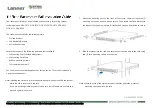
It is possible to connect an external application board to the XE1401SK by using the 50 pins connector JP2. The
pinning of this 50 pins male connector reflects the pinning of the XE1401 (XE1401 - pin 1 = JP2 - pin 1, XE1401 -
pin 2 = JP2 - pin 2 …).
The application board power source at pin 48 has to be set by jumper JP7. Please refer to chapter
5.3
Motherboard Jumper Settings
for more details.
The pinning of the 50 pins 2.54mm male connector is:
50
48
46
44
42
40
38
36
34
32
30
28
26
24
22
20
18
16
14
12
10
8
6
4
2
49
47
45
43
41
39
37
35
33
31
29
27
25
23
21
19
17
15
13
11
9
7
5
3
1
VDD_REG
MCLK
NSS
MISO
PCM_DIN
FSYNC
MODE[0]
MODE[2]
RTS
UA_RX
NC1
RADIO_TYPE
CLK_IN
NC3
NC5
RF_OUT[2]
GND
MOSI
SCK
PCM_DOUT
BCLK
VSSD1
MODE[1]
CTS
UA_TX
NCS
VDD_IO_DIG
NC2
RF_IN[1]
NC4
NC6
NC7
RF_OUT[5]
RF_IN[0]
RF_OUT[1]
RF_OUT[4]
RF_IN[3]
NC8
NRESET
VSSD3
GND
RF_IN[2]
RF_OUT[3]
RF_OUT[0]
RF_OUT[6]
VSSD2
NC9
GND
VOUT*
GND
* Output voltage selectable by jumper JP7
Top view of the 50 pins connector JP2 for an external application board
Note! VOUT
is the output voltage present on pin 48, selected by JP7. If JP7 is set to 1.8V the on chip regulator of
the XE1401 will provide the 1.8V. Be sure that the current sunk by the external application board respects the
maximal current draw provided by the various power sources.