MultiMediaCard Product Manual
SanDisk MultiMediaCard Product Manual Rev. 2 © 2000 SANDISK CORPORATION
60
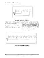
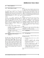
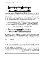
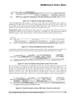
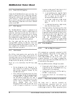
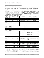
All previous examples dealt with the scenario of the host stopping the data transmission during an
active data transfer. The following two diagrams describe a scenario of receiving the stop transmission
between data blocks. In the first example the card is busy programming the last block while in the
second the card is idle. However, there are still unprogrammed data blocks in the input buffers. These
blocks are being programmed as soon as the stop transmission command is received and the card
activates the busy signal.
Figure 5-17 Stop Transmission Received After Last Data Block. Card is Busy Programming.
Figure 5-18 Stop Transmission Received After Last Data Block. Card Becomes Busy.
Stream Write
—The data transfer starts N
WR
clock cycles after the card response to the sequential write
command was received. The bus transaction is identical to that of a write block command (see
Figure 5-13). As the data transfer is not block oriented, the data stream does not include the CRC
checksum. Consequently the host can not receive any CRC status information from the card. The data
stream is terminated by a stop command. The bus transaction is identical to the write block option when
a data block is interrupted by the stop command (see Figure 5-15).
Erase, Set and Clear Write Protect Timing
—The host must first tag the sectors to erase using the tag
commands (CMD32 - CMD37). The erase command (CMD38), once issued, will erase all tagged sectors.
Similarly, set and clear write protect commands start a programming operation as well. The card will
signal “busy” (by pulling the DAT line low) for the duration of the erase or programming operation. The
bus transaction timings are described in Figure 5-18.
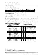
5.10.4 Timing Values
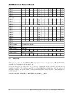
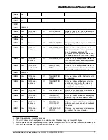
Table 5-12 defines all timing values.
Table 5-12 Timing Values
Min
Max
Unit
N
CR
2
64
Clock Cycles
N
ID
5
5
Clock Cycles
N
AC
2
10 * (TAAC +
NSAC)
Clock Cycles
N
RC
8
-
Clock Cycles
N
CC
8
-
Clock Cycles
N
WR
2
-
Clock Cycles

