background image

Operating Instructions

11-3

Samsung Electronics

ENGLISH

13

13

Getting to Know Your Camcorder

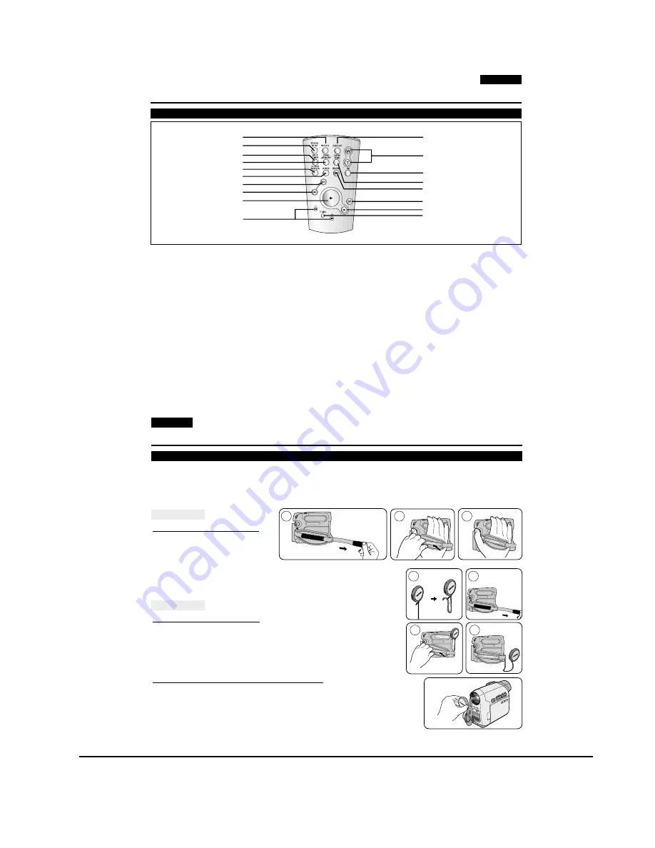
Remote Control (VP-D363(i)/D364W(i)/D365W(i) only)

1. PHOTO Button 

page 57

2. START/STOP Button

3. SELF TIMER Button 

page 38

4. ZERO MEMORY Button 

page 37

5. PHOTO SEARCH Button

6. A.DUB Button 

page 62

7.

√√ 

(FF) Button

8.

œœ 

(REW) Button

9.

(PLAY) Button

10.

œ

❙❙

❙❙

(Direction) Button 

page 59

11. F. ADV Button 

page 60

12.

■ 

(STOP) Button

13.

❙❙

(STILL) Button 

14. SLOW (

) Button

15. DATE/TIME Button

16. X2 Button 

page 60

17. W/T (Zoom) Button

18. DISPLAY Button

1. PHOTO 

2. START/STOP

3. SELF TIMER 

4. ZERO MEMORY

5. PHOTO SEARCH 

6. A.DUB 

7. 

√√ 

(FF) 

9. 

√ 

(PLAY) 

10. 

œ

❙❙

❙❙

(Direction) 

18. DISPLAY

17.  W/T (Zoom)

16. X2

15. DATE/TIME
14. SLOW(

)

13. 

❙❙

(STILL)

11. F. ADV

12. 

■ 

(STOP)

8. 

œœ

(REW) 

ENGLISH

14

14

Preparation

Using the Hand Strap & Lens Cover

It is very important to ensure that the Hand Strap has been correctly adjusted before you begin your recording.
The Hand Strap enables you to:
- Hold the Camcorder in a stable, comfortable position.
- Press the [Zoom] and [Start/Stop] button without having to change the position of your hand.

Hand Strap

Adjusting the Hand Strap

1. Insert the Hand Strap into the Hand

Strap Hook on the front side of 
the Camcorder and pull its end
through the hook.

2. Insert your hand into the Hand Strap and adjust its length for your convenience.
3. Close the Hand Strap.

Lens Cover

Attaching the Lens Cover

1. Hook up the Lens Cover with the Lens Cover Strap as illustrated.
2. Hook up the Lens Cover Strap to the Hand Strap, and adjust it following 

the steps as described for the Hand Strap.

3. Close the Hand Strap.

Installing the Lens Cover after Operation

Press buttons on both sides of the Lens Cover, then insert it to the Camcorder Lens.

1

2

3

1

2

2

3

Summary of Contents for VP-D361

Page 1: ...in Flash Memory ˇ Multi Memory Card Slot Direct Print System PictBridgeTM ˆ LED Light Ø High quality MPEG4 Still image Interpolation Real Wide mode 16 9 WIDE LCD 33X ZOOM USB 2 0 Streaming Manual DIGITAL VIDEO CAMCORDER Merit Character regarding Product SERVICE MANUAL VP D361 i D361W i D362 i D363 i D364W i D365W i ELECTRONICS Samsung Electronics Co Ltd FEB 2006 Printed in Korea AD82 00152A This S...

Page 2: ...sis VP D361 D361I D361WI D361WI 5 2 5 2 Ass y Chassis VP D362 D362I D363 D363I 5 4 5 3 Ass y Chassis VP D364W D364WI D365W D365WI 5 6 5 4 Ass y Left VP D361 D361I D361WI D361WI 5 8 5 5 Ass y Left VP D362 D362I D363 D363I 5 10 5 6 Ass y Left VP D364W D364WI D365W D365WI 5 12 5 7 Ass y Right VP D361 D361I D361WI D361WI 5 14 5 8 Ass y Right VP D362 D362I D363 D363I 5 16 5 9 Ass y Right VP D364W D364W...

Page 3: ...77X Block Diagram 7 4 7 4 IC201 Block Diagram 7 5 7 5 Camera Circuit Block Diagram 7 6 7 6 DV1Chip Block Diagram 7 6 7 7 Audio Video Interface Block Diagram 7 7 7 8 Syscon Servo Block Diagram 7 7 7 9 DCDC Block Diagram 7 8 8 Wiring Diagram 8 1 8 2 9 PCB Diagrams 9 1 9 10 9 1 Main PCB 9 2 9 2 Left PCB 9 6 9 3 LCD PCB 9 6 9 4 Rear PCB 9 7 9 5 Function PCB 9 7 9 6 Jack PCB 9 8 9 7 Front PCB VP D363 D...

Page 4: ...nction Function PCB 10 17 10 17 CVF CVF PCB 10 18 10 18 LCD LCD PCB 10 19 10 19 Front Front PCB VP D363 D363I D364W D364WI D365W D365WI 10 20 11 Operating Instructions and Installation 11 1 11 18 12 Trouble Shooting 12 1 12 12 13 Circuit Operating Descriptions 13 1 13 20 13 1 Summary 13 1 13 2 Digital Camcorder Summary 13 2 13 3 Set Explanation 13 3 13 4 H W demand matter 13 7 14 Reference Informa...

Page 5: ...d Underwriters Laboratories UL 1270 40 7 With the instrument s AC switch first in the ON position and then in the OFF position mea sure from a known earth ground metal water pipe conduit etc to all exposed metal parts of the instrument antennas handle brackets metal cabi nets screwheads metallic overlays control shafts etc especially any exposed metal parts that offer an electrical return path to ...

Page 6: ...nched out of place or frayed wiring Do not change spacing between a component and the printed circuit board Check the AC power cord for damage 5 Components parts and or wiring that appear to have overheated or that are otherwise damaged should be replaced with components parts and or wiring that meet original specifications Additionally determine the cause of overheating and or damage and if neces...

Page 7: ...d lead last 2 The service precautions are indicated or printed on the cabinet chassis or components When servic ing follow the printed or indicated service precau tions and service materials 3 The components used in the unit have a specified flame resistance and dielectric strength When replacing components use components which have the same ratings Components identi fied by shading by or by in th...

Page 8: ...posure of the assem bly 3 Use only a grounded tip soldering iron to solder or unsolder ESD devices 4 Use only an anti static solder removal devices Some solder removal devices not classified as anti static can generate electrical charges suffi cient to damage ESD devices 5 Do not use freon propelled chemicals These can generate electrical charges sufficient to damage ESD devices 6 Do not remove a ...

Page 9: ...ter ø 27 Size dot number 2 5 inch 112K LCD Screen Method TFT LCD Viewfinder Color LCD Video output 1 Vp p 75Ω terminated S video output Y 1Vp p 75Ω C 0 286Vp p 75Ω Audio output 7 5dBs 600Ω terminated DV input output 4pin special in out connector USB output mini B type connector External mic ø 3 5 stereo Power source DC 8 4V lithium lon Battery Pack 7 4V Power Source type Lithium lon Battery Pack P...

Page 10: ...200X 30X 1200x CCD 680K 680K LCD 2 5 112K 2 5 112K Viewfinder Color Color Audio 12 16b PCM 12 16b PCm Image Stabilizer DIS DIS IEEE1394 In Out In OUt USB USB 2 0 USB 2 0 JPEG Recording 800 X 600 800 X 600 Battery Pack SB LSM80 SB LSm80 Carrying Case Tape X X X X S Cable Scart Jack X X X X UV Coating Color UV Coating UV Coating 2 2 Chassis Product Specification ...

Page 11: ...r AD43 00136A AD44 00090A Model Standard of VP D363 XEG Model Standard of VP D363 XEG Model Standard of VP D363 XEG AD39 00077A AC Cord Model Standard of VP D363 XEG AD39 00119A Audio Video Cable Model Standard of VP D363 XEG AD68 00970H Instruction Book Model Standard of VP D363 XEG AD43 10130H Lithium Battery Model Standard of VP D363 XEG AD39 00073A USB Cable ...

Page 12: ... Electronics Description Fig Description Parts No Remark Software Cd Lens Cover AD46 00061A AD46 00082A AD97 10686A Model Standard of VP D363 XEG Model Standard of VP D363 XEG Model Standard of VP D363 XEG AD72 00049A Lens Cover Strap ...

Page 13: ...nishing each adjustment step Ø In order to exit the adjustment mode disconnect the power source 2 Function of each buttons on the Set Key Buttons Description PHOTO Button push Confirm Stores changed value in the adjustment and auto adjustment mode ZOOM Lever Right Data Up Changes data in the adjustment state ZOOM Lever Left Data Down EASY Q Mode Up Changes mode DISPLAY Mode Down Table 3 1 3 How to...

Page 14: ...necting the power source Fig 3 2 Player Mode Back VCR ADJ CAM ADJ CAM DISP LCDCVF AJD DSP WRITE VCRADJ EPR EVR 800 OO OO B 00000 R 00000 BER 0 0E 00 1394 OFF AVIN OFF Indicates current adjustment item Adjustment value For Engineering Mode Stored value Fig 3 3 3 1 2 VCR Adjustment Œ Get into VCR ADJUST mode Move to the VCR ADJUST address 858 ˇ Play standard tape and Head Switching Position will be ...

Page 15: ...M and Camera Main PCB Œ Lens Zoom Track Zoom VR Center ˇ Auto HALL Auto IRIS ˆ Auto White Balance indoor Ø Auto White Balance outdoor 3 2 1 Adjustment Preparation 1 Before you start Œ Use the buttons on the CAMCORDER when adjusting Camera When changing the adjustment item please press the EASY Q or DISPLAY buttons on the Set ˇ You can chage the adjustment value to press macro button or c nite butt...

Page 16: ...ears as shown Fig 3 5 the adjustment mode has been activated successfully ˇ Move the Zoom Lever to highlight CAM ADJ and push the PHOTO Button Monitor OSD shows Fig 3 6 Then Camera adjustment mode has been activated successfully STEP 3 In order to complete the adjustment the power must be reset This can be done by disconnecting and reconnecting the power source Fig 3 5 Player Mode Back VCR ADJ CAM...

Page 17: ...D shows OK after finishing the initalize Show Fig 3 8 2 Lens Zoom Track Caution For whole zoom range it shall be in focus The location of a focus lens is moving depending on the location of Zoom Lens During adjusting micom measures the focus location from a near distance to a long Œ Camera is set to E E mode Set the Focus chart ˇ Center the camera about 3m from a focus chart which should be placed...

Page 18: ...ue with an iris closed Store max and min value of in 00BC 00BD and 00BB respectively ˆ The OSD shows OK after finishing the adjustment Show Fig 3 8 6 Auto White Balance indoor Œ Camera mode 3100 K gray scale chart Connect a video output terminal to a vectorscope and a TV ˇ Press the EASY Q Mode Up DISPLAY Mode Down buttons so that OSD shows 0D4 XX XX Ensure that camera picks up image 40µs on 3100 ...

Page 19: ... Adjustments 3 7 Samsung Electronics EEPROM Data Intialize Lens Zoom Track Zoom VR Center Auto HALL Auto IRIS Level Auto White Balance indoor Auto White Balance outdoor Fig 3 8 When 0DE is not adjusted adjust by 0D0 ...

Page 20: ... and push the PLAY Key Cover the Top End sensor with black tape because they do not operate Note For the removal of the Housing Ass y refer to 4 2 2 page 4 6 SWITCH C IN Connceted the Recorder Circuit Fig 3 9 3 3 2 Setting Mechanical Mode Without Recorder Circuit 1 Set the power supply output to approx 3V 5V 2 Choose the polarity depending on whether load ing or unloading 3 Supply the voltage to t...

Page 21: ...counterclockwise by hand Note Do not rotate the motor by power or rotate the Upper Drum assembly clockwise Also the Head tip will be damaged if the lens tissue is moved in a perpendicular direction Be sure to follow these instructions when cleaning the Drum Ass y 2 Cleaning of Tape Path Œ In EJECT mode clean the tape path system from Pole Tension P1 through Pole Review P8 Pinch Roller and Capstan ...

Page 22: ...e tip of a Ø 2mm stick as shown in Fig 3 11 Table 3 5 Fig 3 12 O Cleaning Oil Confirmation Tape path system D R I V I N G S Y S T E M Never let oil get on to the tape path surface Maintenance checks Hours of use H Remark 500 1000 1500 2000 2500 3000 3500 4000 4500 5000 Cleaning of tape path O O O O O O O O O O Cleaning and degaussing of drum ass y O O O O O O O O O O Capstan Shaft Gear Capstan Gea...

Page 23: ...etween external surface of Holder Loading and extenal diamater of Arm Tension is 0 7 0 3mm Fig 3 12 ˇ If necessary proceed to step 4 If the Arm Tension Œ is located inside or right the position specified adjust the Cap Adjust Œ toward arrow A If it is located outside or left adjust toward arrow B Note Check if the Arm Tension can be moved toward arrow C in PB mode 3 Reassembly Œ For the removal of...

Page 24: ...B REV Torque check 1 Set up the cassette torque tape 2 Set to CAMERA mode Push the EDIT button and check that the torque value of Reel T is 9 3g cm 3 Push the EDIT button and check that the torque value of Reel S is 15 3g cm 4 If necessary replace the defective Reel Disk S T Ass y 3 3 4 d Reel Table Height Check 1 Removal Œ For the removal of the Housing Ass y refer to 4 2 2 page 4 6 For the remov...

Page 25: ...serve the PB RF signal and Head Switching Pulse on an oscilloscope ˇ Play back the alignment tape Check that the waveform of the RF signal is flat at both inlet and outlet A in Fig 3 15 If not flat B or C in Fig 3 15 do adjustments 3 3 5 b through 3 3 5 d RF Signal Pin 3 of CNR02 Head Switching Pin 2 of CNR02 1 2 3 4 5 6 7 8 9 10 11 12 13 14 15 16 17 18 CNR02 Fig 3 16 Rear PCB Top Side ...

Page 26: ...lignment tape and confirm that the tape is not twisted between the Guide Roller T and Capstan If the tape is twisted turn P8 Fig 3 18 Set to REV mode and observe the outlet waveform of PB RF signal Fig 3 19 ˇ If the outlet waveform is out of spec turn P8 counterclockwise and redo steps 1 and 2 P6 P3 MOTOR CAPTAN P8 Fig 3 19 DEFECTIVE CORRECT Fig 3 20 P4 P6 P7 P8 P9 P3 P2 P1 Fig 3 18 A B C INLET OU...

Page 27: ...rm Fig 3 21 2 CUE and REV Check Œ Playback the alignment tape and set to REV mode Confirm that the waveform peaks have a uniform Pitch Fig 3 22 A If the track pitch is not uniform do section 3 3 5 b Tracking adjustment and 3 3 5 c P8 adjustment Set to CUE mode Confirm that the waveform peaks still have a uniform pitch Fig 3 22 B If the track pitch is not uniform do section 3 3 5 b Tracking Adjustm...

Page 28: ...around the Pinch Roller Fig 3 23 ˇ Run the tape in CUE REV and FF REW modes then playback Confirm the waveform of PB RF signal rises flat within 3 seconds Also confirm that the tape is not twisted or curled around the Pinch Roller Repeat steps 2 and 3 4 Tape Path Check Œ In CUE and REV modes check that the tape is not curled around the P3 P6 upper flange and P8 upper Lower flanges P6 P3 MOTOR CAPS...

Page 29: ...ssembly 4 1 Cabinet and PCB Fig 4 1 Ass y Front Removal 4 1 1 Ass y Front Removal 1 Remove 4 Screws Œ ˇ 2 Remove Mic harness Œ 1 SCREW M 1 7 X 4 W MIC HARNESS 1 SCREW M 1 7 X 5 B ˇ 2 SCREWS T 1 7 X 5 B CAUTION Be careful while pulling Mic Harness ...

Page 30: ... Œ ˇ 2 Pull bottom side of Ass y left ˆ gently 3 Ø Pull top side of Ass y left ˆ upward separate from Ass y right Check screw ˇ is removed before pulling ˆ Ass y left upward 4 Remove FFC From Main PCB ˇ 1 SCREW M 1 7 X 5 B ˆ ASS Y LEFT Ø Œ 3 SCREWS M 1 7 X 5 B 1 SCREW M 1 7 X 5 B FFC CAUTION FPC Must be remove with care ...

Page 31: ... Removal 1 Open Cover li battery Œ 2 Remove 2 Screws 3 Open Cover DC jack ˇ 4 Disconnect Board to board connector Which is connecting PCB Rear and Main PCB 5 Remove Ass y rear ˆ by indicated direction 2 SCREWS M 1 7 X 5 B Œ COVER LI BATTERY ˇ COVER DC JACK ˆ ASS Y REAR BOARD TO BOARD CONNECOTOR ...

Page 32: ... Ass y Lens Removal 4 1 4 Ass y Lens Removal 1 Remove 2 Screws Œ 2 Disconnect Board to Board Connector Which is connecting PCB CCD and Main PCB 3 Remove Ass y lens ˇ by Indicated direction Œ 2 SCREW M 1 7 X 3 B ˇ ASS Y LENS DISCONNECT BOARD TO BOARD CONNECTOR ...

Page 33: ...lectronics Fig 4 5 Main PCB Removal 4 1 5 Main PCB Removal 1 Remove 1 FFC Œ 5 FPC 2 Remove 4 screw ˇ 3 Remove Main PCB from Ass y right by indicated dircection MAIN PCB FFC ˇ 1 SCREW M 1 7 X 3 B Œ FPC CAUTION FPC FFC Must be remove with care ...

Page 34: ... Ass y Main Deck Removal 4 1 6 Ass y Main Deck Removal 1 Remove 4 Screw Œ 2 Open Cover Housing indicated direction while pushing Knob tape eject ˇ downward 3 Pull Ass y main deck downward Œ 4 SCREWS M 1 4 X 5 B ASS Y MAIN DECK COVER HOUSING ˇ KNOB TAPE EJECT ˇ ...

Page 35: ...s 1 Set the power supply output to approximately 3V 5V and connect it to the Motor Loading 2 Choose the polarity depending on whether loading or unloading See Table 4 1 3 Supply the voltage to the Motor Loading Fig 4 7 Loading and Unloading A B Movement of Chassis _ Loading _ Unloading Table 4 1 A B 4 2 Deck ...

Page 36: ... 1 Push the Lever see arrow A Detail A turn the Lever Lock Œ in the direction of arrow B and open the Housing Ass y 2 Separate the Hook L and Hook R and then lift it 3 Separate the Shape of Pin L and R ˆ from Cam Parts Ø of Sub Chassis and then lift the Housing Ass y 4 2 2 b Reassembly 1 Mount the Shape of Pin L and R ˆ to Cam Parts Ø of Sub Chassis 2 Mount Shape Ô of Arm L pushing them in the dir...

Page 37: ... 2 Screws Œ then lift the Cover Reel Ass y 2 Then lift the Idler Ass y ˇ 4 2 3 b Reassembly 1 Fit the Idler Ass y ˇ into the Pin 2 Mount the Cover Reel Ass y to the Sub Chassis in the reverse direction of arrow 3 Secure the 2 Screws Œ COVER REEL ASS Y BRAKE S 2SCREWS Œ ˇ IDLER ASS Y Fig 4 9 Cover Reel Ass y Idler Ass y ...

Page 38: ...el Disk S 4 2 4 b Reassembly 1 Mount the Reel Disk S ˆ 2 After pushed Arm Tension Ass y in the direction A and then insert into the Pin Ø 3 Insert the Washer Slit ˇ and then hang the Spring Tension Œ to Sub Chassis Hook and Arm Tension Hook Note 1 When reassembling or dsiassembling position of Spring Tension Œ is same Note 2 When moving inspecting must be inspect Back Tension Note 3 When reassembl...

Page 39: ...assis Ass y from Main Chassis ˇ Fig 4 11 Sub Chassis 4 2 5 b Reassembly 1 Insert PinPart of Sub Chassis Ass y to Main Chassis Rail ˆ and then fit the reassembly part of two place to Secure Hole Ø of Main Chassis Ass y ˇ 2 Secure 2 Screws Œ Note 1 After assembling with ˇ make sure that Sub Chassis Ass y loads and unloads correctly by applying 3V 5V to the Motor Loading Note 2 When reassembling conf...

Page 40: ...4 2 6 a Disassembly 1 After turned Arm Review Œ in the direction of arrow A and then lift up 2 Lift up the Reel Disk T 3 Lift up the Brake T ˇ ARM REVIEW Œ REEL DISK T BRAKE T ˇ PIN Ø PIN ˆ PIN 4 2 6 b Reassembly 1 Insert Brake T ˇ to Pin Ø 2 Insert Reel Disk T to Pin ˆ 3 Insert Arm Review Œ to Pin state of turning in the direction of arrow A Fig 4 12 Arm Review Reel Disk T Brake T ...

Page 41: ...he Drum Œ 1 Remove 1 Screw Œ and then remove the Spring Plate Drum 2 Lift up the Drum ˇ 3 Remove 1 Screw and then lift up the Holder FPC ˆ 4 2 7 b Reassembly 1 Mount and insert the Drum ˇ to the Bosses of base Drum Ø 2 Insert the Spring Plate Drum and secure the 1 Screw Œ 3 Insert the Holder FPC ˆ and secure the 1 Screw DRUM ˇ HOUSING LOCK L BASE DRUM 1 SCRE W ˆ HOLDER FPC Ø 2 BOSSES SPRING PLATE ...

Page 42: ...ler S ˇ and T 3 SCREWS Œ GUIDE ROLLER S ˇ POLE BASE S ˆ POLE BASE T Ø GUUIDE ROLLER T GUIDE RAIL ASS Y MAIN CHASSIS 4 2 8 b Reassembly 1 Assembly the Guide Roller S ˇ and T as turn to countclock wise to the Pole Base S ˆ and T Ø 2 After Pole Base S ˆ and T Ø unloading mode and then assemble Guide Rail Ass y to the Main Chassis and secure the 3 Screws Œ Note 1 When removing and reassembling Guide R...

Page 43: ...After assemble and fit Gear Tension Ø Gear Cam Main to assemble point and then secure the 2 Screws ˆ 2 Insert Hook of Motor Loading Ass y to assemble point of Main Chassis and then secure the 1 Screw 3 After assemble FPC to Motor and then weld pt welding 2 parts Œ Note 1 When reassembling confirm that pin of Slide Main insert into Cam of Gear Cam Main 2 SCREWS ˆ GEAR CAM MAIN 1 SCREW Ø GEAR TENSIO...

Page 44: ...apstan Arm Pinch Roller Slide Main LeverEject 2 2 SCREWS SLIDE MAIN MAIN CHASSIS MOTOR CAPSTAN ˇ WASHER SLIT Ø ARM PINCH ROLLER SPRING LEVER PINCH LEVER EJECT ˆ MAIN CHASSIS HOOK 4 2 10 a Disassembly Note 1 When removing and reassembling be careful not to giss the Gear Part Note 2 When removing and reassembling be careful not to touch the hand in the pinch Roller Protection contamination 1 Remove ...

Page 45: ...apstan 2 Separate the Timing Belt ˇ lift the Gear Pully Fig 4 16 Gear Pully Timing Belt Gear Capstan WASHER SLIT Œ GEAR PULLY ˇ TIMING BELT GEAR CAPSTAN 4 2 11 b Reassembly 1 Mount the Gear Pully and hang the Belt Timming ˇ on the Gear Pully 2 Hang the Timing Belt ˇ to the upper gear of the Gear Capstan and mount the Gear Capstan 3 Assemble the Washer Slit Œ ...

Page 46: ...4 18 Disassembly and Reassembly Samsung Electronics MEMO ...

Page 47: ... D365WI 5 12 5 7 Ass y Right VP D361 D361I D361W D361WI 5 14 5 8 Ass y Right VP D362 D362I D363 D363I 5 16 5 9 Ass y Right VP D364W D364WI D365W D365WI 5 18 5 10 Ass y LCD VP D361 D361I D361W D361WI 5 20 5 11 Ass y LCD VP D362 D362I D363 D363I 5 22 5 12 Ass y LCD VP D364W D364WI D365W D365WI 5 24 5 13 Ass y Case Left VP D363 D363I D364W D364WI D365W D365WI 5 26 5 14 Ass y Case Right 5 27 5 15 Ass ...

Page 48: ...Parts List 5 2 Samsung Electronics 5 1 Ass y Chassis VP D361 D361I D361W D361WI C352 P001 P180 C806 P052 C594 C314 C201 M001 W122 M 1 4 X 5 B W126 M 1 7 X 4 B W126 M 1 7 X 4 B W126 M 1 7 X 4 B S N A Service Not Available ...

Page 49: ...J 1 SA VP D361 XEU AD92 00025F ASSY PCB MAIN BOARD VP D361I XSG DRAGON2 PJ 1 SA VP D361I MEA AD92 00025F ASSY PCB MAIN BOARD VP D361I XSG DRAGON2 PJ 1 SA VP D361I SEA AD92 00025F ASSY PCB MAIN BOARD VP D361I XSG DRAGON2 PJ 1 SA VP D361I XSA AD92 00025F ASSY PCB MAIN BOARD VP D361I XSG DRAGON2 PJ 1 SA VP D361I XSH AD92 00025F ASSY PCB MAIN BOARD VP D361I XSG DRAGON2 PJ 1 SA VP D361I XST AD92 00025F...

Page 50: ...rts List 5 4 Samsung Electronics 5 2 Ass y Chassis VP D362 D362I D363 D363I C352 P005 P001 P180 C806 P052 C594 C314 C201 M001 W122 M 1 4 X 5 B W126 M 1 7 X 4 B W126 M 1 7 X 4 B W126 M 1 7 X 4 B S N A Service Not Available ...

Page 51: ...1 SA VP D363I CHN AD97 10587B ASSY PCB MAIN BOARD DRAGON2 PJ VP D363 XEU MAIN PAL 1 SA VP D363 XEE AD97 10587B ASSY PCB MAIN BOARD DRAGON2 PJ VP D363 XEU MAIN PAL 1 SA VP D363 XEG AD97 10587B ASSY PCB MAIN BOARD DRAGON2 PJ VP D363 XEU MAIN PAL 1 SA VP D363 XEO AD97 10587B ASSY PCB MAIN BOARD DRAGON2 PJ VP D363 XEU MAIN PAL 1 SA VP D363 XET AD97 10587B ASSY PCB MAIN BOARD DRAGON2 PJ VP D363 XEU MAI...

Page 52: ...s List 5 6 Samsung Electronics 5 3 Ass y Chassis VP D364W D364WI D365W D365WI C352 P005 P001 P180 C806 P052 C594 C314 C201 M001 W122 M 1 4 X 5 B W126 M 1 7 X 4 B W126 M 1 7 X 4 B W126 M 1 7 X 4 B S N A Service Not Available ...

Page 53: ...XSG DRAGON2 PJ 1 SA VP D365WI SEA AD92 00025R ASSY PCB MAIN BOARD VP D365WI XSG DRAGON2 PJ 1 SA VP D365WI XSA AD92 00025R ASSY PCB MAIN BOARD VP D365WI XSG DRAGON2 PJ 1 SA VP D365WI XSH AD92 00025R ASSY PCB MAIN BOARD VP D365WI XSG DRAGON2 PJ 1 SA VP D365WI XST AD92 00025U ASSY PCB MAIN BOARD VP D365WI CHN DRAGON2 PJ 1 SA VP D365WI CHN AD92 00025T ASSY PCB MAIN BOARD VP D364W XEU DRAGON2 PJ 1 SA V...

Page 54: ...d View and Parts List 5 8 Samsung Electronics 5 4 Ass y Left VP D361 D361I D361W D361WI W226 T 1 7 X 6 B P091 P004A P247 C849 FL617 P054 P003 W126 T 1 7 X 4 B W126 T 1 7 X 4 B C843 S N A Service Not Available ...

Page 55: ...LAT 30V 80 40mm 40P 0 5mm UL2 1 SA P003 AD92 00020A ASSY PCB LEFT BOARD SC D263 DRAGON2 PJ N 1 SA P004A AD97 10590A ASSY PCB FUNCTION BOARD DRAGON2 PJ SC D3 1 SA P054 AD97 04289A ASSY SPEAKER D5 PJ G 17S08 0823 1 SA P091 AD97 10691C ASSY CASE LEFT ASSY DRAGON2 PJ NO MEMORY 1 SA P247 AD97 10796E ASSY COVER TOP ASSY DRAGON2 PJ UV O MEM 1 SA W126 6003 001300 SCREW TAPTITE CH B M1 7 L4 ZPC BLK SW 5 SA...

Page 56: ...d View and Parts List 5 10 Samsung Electronics 5 5 Ass y Left VP D362 D362I D363 D363I W226 T 1 7 X 6 B P091 P004A P247 C849 FL610 FL617 P054 P003 W126 T 1 7 X 4 B W126 T 1 7 X 4 B S N A Service Not Available ...

Page 57: ...LAT 30V 80 40mm 40P 0 5mm UL20696 1 SA VP D362 XEE 3809 001782 FFC CABLE FLAT 30V 80 40mm 40P 0 5mm UL20696 1 SA VP D362 XEG 3809 001782 FFC CABLE FLAT 30V 80 40mm 40P 0 5mm UL20696 1 SA VP D362 XEO 3809 001782 FFC CABLE FLAT 30V 80 40mm 40P 0 5mm UL20696 1 SA VP D362 XET 3809 001782 FFC CABLE FLAT 30V 80 40mm 40P 0 5mm UL20696 1 SA VP D362 XEU P003 AD92 00020A ASSY PCB LEFT BOARD SC D263 DRAGON2 ...

Page 58: ...ed View and Parts List 5 12 Samsung Electronics 5 6 Ass y Left VP D364W D364WI D365W D365WI W226 T 1 7 X 6 B P091 P004A P247 C849 FL610 P054 P003 W126 T 1 7 X 4 B W126 T 1 7 X 4 B S N A Service Not Available ...

Page 59: ...5mm UL2 1 SA P003 AD97 10589A ASSY PCB LEFT BOARD DRAGON2 PJ SC D366 L 1 SA P004A AD97 10590A ASSY PCB FUNCTION BOARD DRAGON2 PJ SC D3 1 SA P054 AD97 04289A ASSY SPEAKER D5 PJ G 17S08 0823 1 SA P091 AD97 10691D ASSY CASE LEFT ASSY DRAGON2 PJ MULTI MEM 1 SA P247 AD97 10796A ASSY COVER TOP DRAGON2 PJ UV X 1 SA W126 6003 001300 SCREW TAPTITE CH B M1 7 L4 ZPC BLK SW 5 SA W226 6003 001148 SCREW TAPTITE...

Page 60: ...ded View and Parts List 5 14 Samsung Electronics 5 7 Ass y Right VP D361 D361I D361W D361WI C049 W206 M 1 7 X 3 B W206 M 1 7 X 3 B W206 M 1 7 X 3 B W206 M 1 7 X 3 B C047 C012 C010 P055 W126 T 1 7 X 4 B C014 ...

Page 61: ...SY LINK HOUSING ASSY DRAGON2 PJ 1 SA C014 AD97 10795A ASSY BELT GRIP ASSY DRAGON2 PJ SCD6550 1 SA C047 AD63 00897A COVER HOUSING DRAGON2 PJ ABS95HB T2 1 SA C049 AD64 01471A KNOB TAPE EJECT DRAGON2 PJ ABS94HB T1 W5 1 SA P055 AD97 10818C ASSY JACK ASSY DRAGON2 PJ MULTI AV USB 1 SA W126 6003 001300 SCREW TAPTITE CH B M1 7 L4 ZPC BLK SW 2 SA W206 6001 001373 SCREW MACHINE PH T0 5 M1 7 L3 0 ZPC 6 SA ...

Page 62: ...oded View and Parts List 5 16 Samsung Electronics 5 8 Ass y Right VP D362 D362I D363 D363I C049 W206 M 1 7 X 3 B W206 M 1 7 X 3 B W206 M 1 7 X 3 B W206 M 1 7 X 3 B C047 C012 C010 P055 W126 T 1 7 X 4 B C014 ...

Page 63: ...ASSY LINK HOUSING ASSY DRAGON2 PJ 1 SA C014 AD97 10795A ASSY BELT GRIP ASSY DRAGON2 PJ SCD6550 1 SA C047 AD63 00897A COVER HOUSING DRAGON2 PJ ABS95HB T2 1 SA C049 AD64 01471A KNOB TAPE EJECT DRAGON2 PJ ABS94HB T1 W5 1 SA P055 AD97 10818A ASSY JACK ASSY DRAGON2 PJ ASSY JACK 1 SA W126 6003 001300 SCREW TAPTITE CH B M1 7 L4 ZPC BLK SW 2 SA W206 6001 001373 SCREW MACHINE PH T0 5 M1 7 L3 0 ZPC 6 SA ...

Page 64: ...ed View and Parts List 5 18 Samsung Electronics 5 9 Ass y Right VP D364W D364WI D365W D365WI C049 W206 M 1 7 X 3 B W206 M 1 7 X 3 B W206 M 1 7 X 3 B W206 M 1 7 X 3 B C047 C012 C010 P055 W126 T 1 7 X 4 B C014 ...

Page 65: ...ASSY LINK HOUSING ASSY DRAGON2 PJ 1 SA C014 AD97 10795A ASSY BELT GRIP ASSY DRAGON2 PJ SCD6550 1 SA C047 AD63 00897A COVER HOUSING DRAGON2 PJ ABS95HB T2 1 SA C049 AD64 01471A KNOB TAPE EJECT DRAGON2 PJ ABS94HB T1 W5 1 SA P055 AD97 10818A ASSY JACK ASSY DRAGON2 PJ ASSY JACK 1 SA W126 6003 001300 SCREW TAPTITE CH B M1 7 L4 ZPC BLK SW 2 SA W206 6001 001373 SCREW MACHINE PH T0 5 M1 7 L3 0 ZPC 6 SA ...

Page 66: ...Exploded View and Parts List 5 20 Samsung Electronics 5 10 Ass y LCD VP D361 D361I D361W D361WI L011 L006 L004 C349 L053 L013 W124 M 1 7 X 3 W W118 M 1 4 X 3 B L017 L015 L014 P179 C846 ...

Page 67: ... SA VP D361I MEA AD97 10935A ASSY PCB LCD BOARD DRAGON2 PJ AUO2 5 LCD BOARD 1 SA VP D361I SEA AD97 10935A ASSY PCB LCD BOARD DRAGON2 PJ AUO2 5 LCD BOARD 1 SA VP D361I XEV AD97 10935A ASSY PCB LCD BOARD DRAGON2 PJ AUO2 5 LCD BOARD 1 SA VP D361I XSA AD97 10935A ASSY PCB LCD BOARD DRAGON2 PJ AUO2 5 LCD BOARD 1 SA VP D361I XSH AD97 10935A ASSY PCB LCD BOARD DRAGON2 PJ AUO2 5 LCD BOARD 1 SA VP D361I XS...

Page 68: ...Exploded View and Parts List 5 22 Samsung Electronics 5 11 Ass y LCD VP D362 D362I D363 D363I L011 L006 L004 C349 L053 L013 W124 M 1 7 X 3 W W118 M 1 4 X 3 B L017 L015 L014 P179 C846 ...

Page 69: ... TOP DRAGON2 PJ ABS94HB T1 W51 L71 SIL VP D363 1 SA VP D363 XEO AD61 02343E CASE LCD TOP DRAGON2 PJ ABS94HB T1 W51 L71 SIL VP D363 1 SA VP D363 XET AD61 02343E CASE LCD TOP DRAGON2 PJ ABS94HB T1 W51 L71 SIL VP D363 1 SA VP D363 XEU AD61 02343F CASE LCD TOP DRAGON2 PJ ABS94HB T1 W51 L71 SIL VP D363i 1 SA VP D363I MEA AD61 02343F CASE LCD TOP DRAGON2 PJ ABS94HB T1 W51 L71 SIL VP D363i 1 SA VP D363I ...

Page 70: ...Exploded View and Parts List 5 24 Samsung Electronics 5 12 Ass y LCD VP D364W D364WI D365W D365WI L011 L006 L004 C349 L053 L013 W124 M 1 7 X 3 W W118 M 1 4 X 3 B L017 L015 L014 P179 C846 ...

Page 71: ...T1 W51 L 1 SA L011 AD64 00808A BADGE SAMSUNG ALPHA_PJ AL T0 7 SIL 1 SA L013 AD61 02344A CASE LCD BOTTOM DRAGON2 PJ ABS94HB T1 W5 1 SA L014 AD63 00893A COVER HINGE TOP DRAGON2 PJ ABS94HB T1 W9 1 SA L015 AD63 00894A COVER HINGE BOTTOM DRAGON2 PJ ABS94HB T1 1 SA L017 AD97 10690A ASSY LCD FPC DRAGON2 PJ ASSY LCD FPC 1 SA L053 AD07 00055A LCD PANNEL A027DL01 V0 RAINBOW2 PJ 960 2 1 SA P179 AD97 10677A A...

Page 72: ... 0 8 1 SA C843 AD69 00678B PAD LCD VP D452N PORON T1 0 W4 0 2 SA C844 AD61 02479A SPRING ETC DOOR MULTI DRAGON OASIS SUS 0 2 1 1 4 1 SA C845 AD69 00796A PAD DOOR DRAGON2 PJ PORON T1 W2 L5 BLK 1 SA C877 AD61 02359A BRACKET DOOR MULTI DRAGON2 PJ STS T0 3 W7 L17 1 SA Exploded View and Parts List 5 26 Samsung Electronics 5 13 Ass y Case Left VP D363 D363I D364W D364WI D365W D365WI C843 C877 C844 C635 ...

Page 73: ... PLATE POWER TIGER PJ SUS301 1 2H T0 5 W1 1 SA C020 AD64 01341A LOCKER POWER TIGER PJ POM GREEN 1 SA C022 AD73 00006A RUBBER GUIDE DECK BUTHYL RUB VP D50 3 SA C059 AD61 02353A HOLDER POWER DRAGON2 PJ POM T1 W8 L15 D 1 SA C308 AD61 02047A PLATE SPRING POWER TIGER PJ SUS301 1 2H 1 SA C334 AD63 00933A COVER DC JACK DRAGON2 OASIS URETHAN T1 0 1 SA C399 AD61 02364A PLATE NUT DRAGON2 PJ SECC T0 8 W3 L3 ...

Page 74: ... EVF 1 SA C546 AD63 00892A COVER EYE CUP DRAGON2 PJ ABS94HB T1 W23 1 SA C589 AD61 02186A HOLDER CVF SLIDE RAPIDO2 POM T1 0 W 1 SA C667 AD61 02347A CASE CVF MAIN DRAGON2 PJ ABS94HB T1 1 SA C686 AD64 01472A KNOB CVF DRAGON2 PJ PC T1 W8 L9 D G 1 SA L054 AD97 11057A ASSY UNIT CVF NTSC PAL øÎ DRAGON2 PJ UN 1 SA W126 6003 001300 SCREW TAPTITE CH B M1 7 L4 ZPC BLK SW 1 SA 5 15 Ass y CVF W126 T 1 7 X 4 B ...

Page 75: ... 1 SA VP D361W AD92 00023A ASSY PCB JACK BOARD VP D361 DRAGON2 Mult 1 SA VP D361WI AD97 10591A ASSY PCB JACK BOARD DRAGON2 PJ SC D366 J 1 SA VP D362 AD97 10591A ASSY PCB JACK BOARD DRAGON2 PJ SC D366 J 1 SA VP D362I AD97 10591A ASSY PCB JACK BOARD DRAGON2 PJ SC D366 J 1 SA VP D363 AD97 10591A ASSY PCB JACK BOARD DRAGON2 PJ SC D366 J 1 SA VP D363I AD97 10591A ASSY PCB JACK BOARD DRAGON2 PJ SC D366 ...

Page 76: ...Exploded View and Parts List 5 30 Samsung Electronics 5 17 Ass y Rear W112 T 1 7 X 4 B C041 P101 C015 C044 C045 C306 P009 C850 S N A Service Not Available ...

Page 77: ...4 L5 1 SA C044 AD64 01180B KNOB BATTERY EJECT OMEGA2 PJ 2M ABS 94H 1 SA C045 AD61 02351A HOLDER BATTERY EJECT DRAGON2 PJ POM T1 5 1 SA C306 AD61 01625B SPRING ETC BATTERY EJECT THETA2 PJ SUS30 1 SA C850 AD63 00703A COVER BATTERY B DRAGON PJ ABS 94HB T3 8 1 SA P009 AD97 10588A ASSY PCB REAR BOARD DRAGON2 PJ SC D363 X 1 SA P101 AD97 11093A ASSY CASE REAR ASSY DRAGON2 PJ 1 SA W112 6003 001453 SCREW T...

Page 78: ... View and Parts List 5 32 Samsung Electronics 5 18 Mechanical Parts Main Chassis M010 W105 M011 M013 W106 M019 W107 M018 W101 W104 W103 M022 W106 M012 M202 M023 M017 M024 M203 M416 M014 M015 M020 M021 M026 M016 ...

Page 79: ...LER Mold ETC DD 4 PI 4 1 1 SNA M021 AD61 01483A GUIDE ROLLER DD 4 POM BLACK MOLD T 1 SNA M022 AD61 00558A PLATE S P BASE DD 3 SUS632 CSP T0 15 1 SA M023 AD66 00221A PULLEY BELT TIMING DD 4 POLYURETHAN 0 8 SA AD66 00292A PULLEY BELT TIMING DD 4 POLYURETHAN 0 2 SA M024 AD66 00069A GEAR CAPSTAN DD 3 DYAMID 0 4 28 PCD 1 SA M026 AD66 00219A GEAR PULLEY DD 4 DURACON M90 44 0 3 44 1 SNA M202 6031 001417 ...

Page 80: ...Exploded View and Parts List 5 34 Samsung Electronics 5 19 Mechanical Parts Sub Chassis M030 M033 M037 M203 M036 W101 M042 M041 C353 S302 M032 M035 M038 M034 M043 M044 S310 S N A Service Not Available ...

Page 81: ...7 06401A ASSY ARM TENSION DD 4 ASSY 1 SA M037 AD61 01184A SPRING ETC TENSION DD 4 SUS304 WPB 1 SA M038 AD97 06402A ASSY ARM REVIEW DD 4 ASSY 1 SA M041 AD61 01194A HOUSING LOCK L DD 4 DURACON M90 44DURACO 1 SA M042 AD61 01195A HOUSING LOCK R DD 4 DURACON M90 44 DURA 1 SA M043 AD61 01159A HOLDER BAND DD 4 DURACON M90 44 NA 1 SNA M044 AD69 00425A BAND TENSION DD 4 LUMIRROR WHITE 1 SNA M203 6031 00143...

Page 82: ...Exploded View and Parts List 5 36 Samsung Electronics MEMO ...

Page 83: ...HIP 0 68NF 10 50V X7R TP 10 1 SA VP D361WI XEV C206 2203 006048 C CER CHIP 100nF 10 10V X7R 1005 1 SA VP D361I MEA C206 2203 006048 C CER CHIP 100nF 10 10V X7R 1005 1 SA VP D361I SEA C206 2203 006048 C CER CHIP 100nF 10 10V X7R 1005 1 SA VP D361I XEV C206 2203 006048 C CER CHIP 100nF 10 10V X7R 1005 1 SA VP D361I XSA C206 2203 006048 C CER CHIP 100nF 10 10V X7R 1005 1 SA VP D361I XSH C206 2203 006...

Page 84: ...2203 005627 C CER CHIP 470nF 10 10V X5R 1608 1 SA VP D361I XSH 2203 005627 C CER CHIP 470nF 10 10V X5R 1608 1 SA VP D361I XST 2203 005627 C CER CHIP 470nF 10 10V X5R 1608 1 SA VP D361I XTL 2203 005627 C CER CHIP 470nF 10 10V X5R 1608 1 SA VP D361I CHN 2203 005627 C CER CHIP 470nF 10 10V X5R 1608 1 SA VP D361WI XEV C340 2203 000438 C CER CHIP 1nF 10 50V X7R 1005 1 SA C341 2203 000438 C CER CHIP 1nF...

Page 85: ...3 006048 C CER CHIP 100NF 10 10V X7R TP 100 1 SA CA33 2203 006048 C CER CHIP 100NF 10 10V X7R TP 100 1 SA CA34 2203 006048 C CER CHIP 100NF 10 10V X7R TP 100 1 SA CA35 2203 006048 C CER CHIP 100NF 10 10V X7R TP 100 1 SA CA37 2203 005061 C CER CHIP 100nF 80 20 16V Y5V 10 1 SA CM01 2203 001221 C CER CHIP 0 82NF 10 50V X7R TP 10 1 SA CM03 2203 000278 C CER CHIP 0 01nF 0 5pF 50V C0G 100 1 SA CM04 2203...

Page 86: ... L723 2703 002724 INDUCTOR SMD 10UH 10 2012 1 SA L724 2703 002724 INDUCTOR SMD 10UH 10 2012 1 SA L726 2703 002727 INDUCTOR SMD 4 7UH 20 2012 1 SA L727 2703 002727 INDUCTOR SMD 4 7UH 20 2012 1 SA L729 2703 002723 INDUCTOR SMD 22UH 10 2012 1 SA L730 2007 000552 R CHIP 20ohm 5 1 10W TP 1608 1 SA L732 2703 002723 INDUCTOR SMD 22UH 10 2012 1 SA L734 2703 002724 INDUCTOR SMD 10UH 10 2012 1 SA LM01 2007 ...

Page 87: ...1 16W TP 1005 1 SA VP D361WI XEV R202 2007 000138 R CHIP 100ohm 5 1 16W TP 1005 1 SA R204 2007 007311 R CHIP 22Kohm 1 1 16W TP 1005 1 SA R205 2007 001333 R CHIP 18KOHM 5 1 16W TP 1005 1 SA R206 2007 002970 R CHIP 56ohm 5 1 16W TP 1005 1 SA R207 2007 000171 R CHIP 0ohm 5 1 16W TP 1005 1 SA R208 2007 000171 R CHIP 0ohm 5 1 16W TP 1005 1 SA R209 2007 000140 R CHIP 1Kohm 5 1 16W TP 1005 1 SA R210 2007...

Page 88: ...IP 68Kohm 5 1 16W TP 1005 1 SA R321 2007 000162 R CHIP 100Kohm 5 1 16W TP 1005 1 SA R327 2007 001325 R CHIP 3 3Kohm 5 1 16W TP 1005 1 SA R332 2007 000138 R CHIP 100ohm 5 1 16W TP 1005 1 SA R333 2007 000138 R CHIP 100ohm 5 1 16W TP 1005 1 SA R334 2007 000138 R CHIP 100ohm 5 1 16W TP 1005 1 SA R335 2007 000138 R CHIP 100ohm 5 1 16W TP 1005 1 SA R336 2007 000138 R CHIP 100ohm 5 1 16W TP 1005 1 SA R33...

Page 89: ...07 000162 R CHIP 100Kohm 5 1 16W TP 1005 1 SA R550 2007 000140 R CHIP 1Kohm 5 1 16W TP 1005 1 SA R5501 2007 000171 R CHIP 0ohm 5 1 16W TP 1005 1 SA R5502 2007 000171 R CHIP 0ohm 5 1 16W TP 1005 1 SA R5503 2007 000171 R CHIP 0ohm 5 1 16W TP 1005 1 SA R5504 2007 000171 R CHIP 0ohm 5 1 16W TP 1005 1 SA R5505 2007 000171 R CHIP 0ohm 5 1 16W TP 1005 1 SA R551 2007 000162 R CHIP 100Kohm 5 1 16W TP 1005 ...

Page 90: ...hm 5 1 16W TP 1005 1 SA RM100 2007 000162 R CHIP 100Kohm 5 1 16W TP 1005 1 SA RM101 2007 000162 R CHIP 100Kohm 5 1 16W TP 1005 1 SA RM102 2007 000172 R CHIP 10ohm 5 1 16W TP 1005 1 SA RM11 2007 000140 R CHIP 1Kohm 5 1 16W TP 1005 1 SA RM12 2007 000138 R CHIP 100ohm 5 1 16W TP 1005 1 SA RM127 2007 000162 R CHIP 100Kohm 5 1 16W TP 1005 1 SA RM128 2007 000162 R CHIP 100Kohm 5 1 16W TP 1005 1 SA RM134...

Page 91: ... 1 SA VP D361I MEA 2007 000171 R CHIP 0ohm 5 1 16W TP 1005 1 SA VP D361I SEA 2007 000171 R CHIP 0ohm 5 1 16W TP 1005 1 SA VP D361I XEV 2007 000171 R CHIP 0ohm 5 1 16W TP 1005 1 SA VP D361I XSA 2007 000171 R CHIP 0ohm 5 1 16W TP 1005 1 SA VP D361I XSH 2007 000171 R CHIP 0ohm 5 1 16W TP 1005 1 SA VP D361I XST 2007 000171 R CHIP 0ohm 5 1 16W TP 1005 1 SA VP D361I XTL 2007 000171 R CHIP 0ohm 5 1 16W T...

Page 92: ...0 0 1 SA VP D361W XET AD41 00792A PCB LCD DRAGON2 PJ FR4 2L REV 00 0 1 SA VP D361WI XEV BL01 3301 001649 BEAD SMD 180ohm 1608 TP 226ohm 1 SA VP D361 EUR 3301 001649 BEAD SMD 180ohm 1608 TP 226ohm 1 SA VP D361 XEE 3301 001649 BEAD SMD 180ohm 1608 TP 226ohm 1 SA VP D361 XEF 3301 001649 BEAD SMD 180ohm 1608 TP 226ohm 1 SA VP D361 XEG 3301 001649 BEAD SMD 180ohm 1608 TP 226ohm 1 SA VP D361 XEN 3301 00...

Page 93: ... 1 1 SA VP D361I CHN CL04 2203 005774 C CER CHIP 1000nF 80 20 50V Y5V T 1 SA VP D361 EUR 2203 005774 C CER CHIP 1000nF 80 20 50V Y5V T 1 SA VP D361 XEE 2203 005774 C CER CHIP 1000nF 80 20 50V Y5V T 1 SA VP D361 XEF 2203 005774 C CER CHIP 1000nF 80 20 50V Y5V T 1 SA VP D361 XEG 2203 005774 C CER CHIP 1000nF 80 20 50V Y5V T 1 SA VP D361 XEN 2203 005774 C CER CHIP 1000nF 80 20 50V Y5V T 1 SA VP D361 ...

Page 94: ...R 3216 1 SA VP D361W XEF 2203 005619 C CER CHIP 4700nF 10 16V X5R 3216 1 SA VP D361W XEG 2203 005619 C CER CHIP 4700nF 10 16V X5R 3216 1 SA VP D361W XEO 2203 005619 C CER CHIP 4700nF 10 16V X5R 3216 1 SA VP D361W XET 2203 005619 C CER CHIP 4700nF 10 16V X5R 3216 1 SA VP D361WI XEV CL09 2203 005774 C CER CHIP 1000nF 80 20 50V Y5V T 1 SA VP D361 EUR 2203 005774 C CER CHIP 1000nF 80 20 50V Y5V T 1 SA...

Page 95: ... VP D361I XSH 2203 005065 C CER CHIP 1000nF 80 20 10V Y5V 1 1 SA VP D361I XST 2203 005065 C CER CHIP 1000nF 80 20 10V Y5V 1 1 SA VP D361I XTL 2203 005065 C CER CHIP 1000nF 80 20 10V Y5V 1 1 SA VP D361I CHN CL14 2203 005619 C CER CHIP 4700nF 10 16V X5R 3216 1 SA VP D361W XEF 2203 005619 C CER CHIP 4700nF 10 16V X5R 3216 1 SA VP D361W XEG 2203 005619 C CER CHIP 4700nF 10 16V X5R 3216 1 SA VP D361W X...

Page 96: ...D361 XEN 2203 005065 C CER CHIP 1000nF 80 20 10V Y5V 1 1 SA VP D361 XEO 2203 005065 C CER CHIP 1000nF 80 20 10V Y5V 1 1 SA VP D361 XET 2203 005065 C CER CHIP 1000nF 80 20 10V Y5V 1 1 SA VP D361 XEU 2203 005065 C CER CHIP 1000nF 80 20 10V Y5V 1 1 SA VP D361I MEA 2203 005065 C CER CHIP 1000nF 80 20 10V Y5V 1 1 SA VP D361I SEA 2203 005065 C CER CHIP 1000nF 80 20 10V Y5V 1 1 SA VP D361I XEV 2203 00506...

Page 97: ... 1608 1 SA RR12 2007 001198 R CHIP 820ohm 1 1 8W TP 2012 1 SA RR13 2007 001198 R CHIP 820ohm 1 1 8W TP 2012 1 SA RR14 2007 000090 R CHIP 10Kohm 5 1 10W TP 1608 1 SA RR30 2007 000077 R CHIP 470ohm 5 1 10W TP 1608 1 SA RR31 2007 000077 R CHIP 470ohm 5 1 10W TP 1608 1 SA RR32 2007 000076 R CHIP 330ohm 5 1 10W TP 1608 1 SA RR33 2007 000076 R CHIP 330ohm 5 1 10W TP 1608 1 SA RR34 2007 000076 R CHIP 330...

Page 98: ...01 I 0 4 SNA AD33 00055A HEAD DVC A HWHAC1017A FERRITE MIG Y 1 SNA AD33 00056A HEAD DVC B HWHAC1018A FERRITE MIG R 1 SNA AD66 00296A DRUM UPPER FORGING DD 4 AHS OD21 1 SNA AD70 00024A CORE TRANS ROTOR FERRITE 0 9 1 SNA AD97 09129A ASSY MOTOR ROTOR ASSY DD 4 Tesla 1 SNA AD31 00052A ROTOR YOKE DM DD 4 SECC C20 0 5 1 SNA AD61 01475A MAGNET DM DD 3 Nd ƒ Ω Ω 1 SNA AD97 10567A ASSY COVER DRUM ASSY DD 4A...

Page 99: ...ORD AA E6A M4206 M4206 250V 1 SA VP D361W XEF AD39 00077A POWER CORD AA E6A M4206 M4206 250V 1 SA VP D361W XEG AD39 00077A POWER CORD AA E6A M4206 M4206 250V 1 SA VP D361W XEO AD39 00077A POWER CORD AA E6A M4206 M4206 250V 1 SA VP D361W XET AD39 00077A POWER CORD AA E6A M4206 M4206 250V 1 SA VP D361WI XEV AD39 00119A CBF CABLE MULTI CABLE A9108642 VP D 1 SA AD43 00136A BATTERY PACK SB LSM80 EXP SO...

Page 100: ...6 R CHIP 20Kohm 5 1 8W TP 2012 1 SA R71 2007 000300 R CHIP 10Kohm 5 1 8W TP 2012 1 SA R72 2007 000582 R CHIP 22Kohm 1 1 8W TP 2012 1 SA R74 2007 001205 R CHIP 82Kohm 1 1 8W TP 2012 1 SA R76 2005 000102 R WIRE WOUND 0 1ohm 1 1W AA TP 4 5 1 SA R77 2007 000068 R CHIP 470Kohm 5 1 8W TP 2012 1 SA R79 2007 001067 R CHIP 6 8Kohm 1 1 8W TP 2012 1 SA R80 2007 000477 R CHIP 1Mohm 5 1 8W TP 2012 1 SC VR50 21...

Page 101: ...0 10V X7R TP 100 1 SA C221 2203 000254 C CER CHIP 10nF 10 16V X7R 1005 1 SA C222 2203 006006 C CER CHIP 0 005NF æ0 25PF 50V C0G 1 SA C223 2203 006006 C CER CHIP 0 005NF æ0 25PF 50V C0G 1 SA C224 2203 006006 C CER CHIP 0 005NF æ0 25PF 50V C0G 1 SA C225 2203 006006 C CER CHIP 0 005NF æ0 25PF 50V C0G 1 SA C227 2203 005923 C CER CHIP 1000NF 20 6 3V X5R TP 1 1 SA C228 2203 006048 C CER CHIP 100nF 10 10...

Page 102: ... C505 2203 000254 C CER CHIP 10nF 10 16V X7R 1005 1 SA C506 2203 000714 C CER CHIP 3 3nF 10 50V X7R TP 100 1 SA C507 2203 006006 C CER CHIP 0 005NF æ0 25PF 50V C0G 1 SA C508 2203 000278 C CER CHIP 0 01nF 0 5pF 50V C0G 100 1 SA C509 2203 000254 C CER CHIP 10nF 10 16V X7R 1005 1 SA C510 2404 001020 C TA CHIP 10uF 20 10V GP TP 3216 1 SA C511 2203 005922 C CER CHIP 4700NF 20 6 3V X5R TP 2 1 SA C512 22...

Page 103: ...X7R TP 100 1 SA CMP27 2203 006048 C CER CHIP 100NF 10 10V X7R TP 100 1 SA CMP28 2203 006048 C CER CHIP 100NF 10 10V X7R TP 100 1 SA CN101 3708 001842 CONNECTOR FPC FFC PIC 7P 0 5MM SMD 1 SA CN301 3708 002203 CONNECTOR FPC FFC PIC 40P 0 5mm SMD 1 SA VP D362 XEE 3708 002203 CONNECTOR FPC FFC PIC 40P 0 5mm SMD 1 SA VP D362 XEG 3708 002203 CONNECTOR FPC FFC PIC 40P 0 5mm SMD 1 SA VP D362 XEO 3708 0022...

Page 104: ...SA PS701 3601 001331 FUSE SURFACE MOUNT 32V 1 25A SLOW B 1 SA PS702 3601 001331 FUSE SURFACE MOUNT 32V 1 25A SLOW B 1 SA Q111 0501 002128 TR SMALL SIGNAL KTC4075 NPN 100mW U 1 SA Q112 0501 002128 TR SMALL SIGNAL KTC4075 NPN 100mW U 1 SA Q201 0501 000225 TR SMALL SIGNAL 2SC4617 NPN 200mW E 1 SA VP D362I XEV 0501 000225 TR SMALL SIGNAL 2SC4617 NPN 200mW E 1 SA VP D363I MEA 0501 000225 TR SMALL SIGNA...

Page 105: ...01306 R CHIP 150ohm 5 1 16W TP 1005 1 SA R216 2007 000142 R CHIP 2 7KOHM 5 1 16W TP 1005 1 SA R217 2007 000164 R CHIP 150KOHM 5 1 16W TP 1005 1 SA R220 2007 000171 R CHIP 0ohm 5 1 16W TP 1005 1 SA R2200 2007 000171 R CHIP 0ohm 5 1 16W TP 1005 1 SA R2201 2007 000171 R CHIP 0ohm 5 1 16W TP 1005 1 SA R221 2007 000170 R CHIP 1Mohm 5 1 16W TP 1005 1 SA R222 2007 008391 R CHIP 6 34KOHM 1 1 16W DA TP 100...

Page 106: ...57 R CHIP 47Kohm 5 1 16W TP 1005 1 SA R418 2007 000155 R CHIP 27Kohm 5 1 16W TP 1005 1 SA R428 2007 000483 R CHIP 1OHM 5 1 8W TP 2012 1 SA R430 2007 000483 R CHIP 1OHM 5 1 8W TP 2012 1 SA R436 2007 000775 R CHIP 33KOHM 5 1 16W TP 1005 1 SA R437 2007 000775 R CHIP 33KOHM 5 1 16W TP 1005 1 SA R443 2007 000159 R CHIP 56Kohm 5 1 16W TP 1005 1 SA R444 2007 000159 R CHIP 56Kohm 5 1 16W TP 1005 1 SA R449...

Page 107: ...0Kohm 5 1 16W TP 1005 1 SA R5602 2007 000162 R CHIP 100Kohm 5 1 16W TP 1005 1 SA R561 2007 000162 R CHIP 100Kohm 5 1 16W TP 1005 1 SA R562 2007 000162 R CHIP 100Kohm 5 1 16W TP 1005 1 SA R564 2007 000140 R CHIP 1Kohm 5 1 16W TP 1005 1 SA R566 2007 000140 R CHIP 1Kohm 5 1 16W TP 1005 1 SA R567 2007 000162 R CHIP 100Kohm 5 1 16W TP 1005 1 SA R568 2007 000162 R CHIP 100Kohm 5 1 16W TP 1005 1 SA R569 ...

Page 108: ...8Kohm 1 1 16W TP 1005 1 SA RM30 2007 007313 R CHIP 6 8Kohm 1 1 16W TP 1005 1 SA RM303 2007 000148 R CHIP 10Kohm 5 1 16W TP 1005 1 SA RM304 2007 000148 R CHIP 10Kohm 5 1 16W TP 1005 1 SA RM311 2007 000162 R CHIP 100Kohm 5 1 16W TP 1005 1 SA RM32 2007 000171 R CHIP 0ohm 5 1 16W TP 1005 1 SA RM34 2007 000171 R CHIP 0ohm 5 1 16W TP 1005 1 SA RM35 2007 000171 R CHIP 0ohm 5 1 16W TP 1005 1 SA RM40 2007 ...

Page 109: ... 4 7Kohm 5 1 16W TP 1005 1 SA RP315 2007 001325 R CHIP 3 3Kohm 5 1 16W TP 1005 1 SA RP316 2007 000153 R CHIP 22Kohm 5 1 16W TP 1005 1 SA RP317 2007 000157 R CHIP 47Kohm 5 1 16W TP 1005 1 SA RP39 2007 001307 R CHIP 180ohm 5 1 16W TP 1005 1 SA RP40 2007 001307 R CHIP 180ohm 5 1 16W TP 1005 1 SA RP41 2007 000159 R CHIP 56Kohm 5 1 16W TP 1005 1 SA RP42 2007 000159 R CHIP 56Kohm 5 1 16W TP 1005 1 SA RP...

Page 110: ...A CHIP 1UF 20 16V TP 2012 1 SA CLF18 2203 005065 C CER CHIP 1000nF 80 20 10V Y5V 1 1 SA CLF19 2203 005148 C CER CHIP 100nF 10 16V X7R TP 160 1 SA CNLF01 3708 002203 CONNECTOR FPC FFC PIC 40P 0 5mm SMD 1 SA 3708 002203 CONNECTOR FPC FFC PIC 40P 0 5mm SMD 1 SA 3708 002203 CONNECTOR FPC FFC PIC 40P 0 5mm SMD 1 SA 3708 002203 CONNECTOR FPC FFC PIC 40P 0 5mm SMD 1 SA 3708 002203 CONNECTOR FPC FFC PIC 4...

Page 111: ...B 1 SA LBTR2 AD63 00075A TERMINAL LI BATT M1 PJ C5210R H 1 SA LDR01 0601 001419 LED SMD RED 3 2X1 6X1 1MM 660NM 3 1 SA QR01 0504 001102 TR DIGITAL EMD3 NPN PNP 150MW 10K 1 1 SA QR02 0504 000168 TR DIGITAL RN1104 NPN 100mW 47K 47K 1 SA QR03 0504 000168 TR DIGITAL RN1104 NPN 100mW 47K 47K 1 SA QR04 0501 000172 TR SMALL SIGNAL 2SB1121 PNP 500mW P 1 SA QR05 0501 000172 TR SMALL SIGNAL 2SB1121 PNP 500m...

Page 112: ...N M90 44 1 SNA AD66 00062A GEAR WORM MOTOR DD 3 POM 0 3 1 SNA AD66 00209A GEAR WORM LOADING DD 4 POM KT 20 0 1 SNA AD61 02335A STUD GEAR CAM MAIN DD 4A SUSXM7 1 SNA AD67 00210A BRUSH MODE S W DD 4 C5210P H 1 SNA AD61 01163A HOLDER BEARING DD 4 ZDC 1 SNA AD61 01165A PLATE CAPSTAN DD 4 RM T0 5 NAT 1 SNA AD61 01544A POST BASE DRUM DD 4 SUS303 D2 0 L8 1 SNA AD66 00213A DRUM BASE DD 4 AEI501 BLK 1 SNA ...

Page 113: ...OWER CORD AA E6A MP5004A MP5004A 2 1 SA VP D363XEU AD39 00077A POWER CORD AA E6A M4206 M4206 250V 1 SA VP D363I MEA AD39 00077A POWER CORD AA E6A M4206 M4206 250V 1 SA VP D363I SEA AD39 00077A POWER CORD AA E6A M4206 M4206 250V 1 SA VP D363I XTL AD39 00077A POWER CORD AA E6A M4206 M4206 250V 1 SA VP D363I XEV AD39 00080A POWER CORD AA E6A V301C V301C 250V 1 SA VP D363I CHN AD39 00119A CBF CABLE MU...

Page 114: ...DER BATTERY BRM D2 BRM E1 WL 85 1 SA VP D363I XEV AD61 00628A HOLDER BATTERY BRM D2 BRM E1 WL 85 1 SA VP D363I CHN AD61 00628A HOLDER BATTERY BRM D2 BRM E1 WL 85 1 SA VP D363 XEE AD61 00628A HOLDER BATTERY BRM D2 BRM E1 WL 85 1 SA VP D363 XEG AD61 00628A HOLDER BATTERY BRM D2 BRM E1 WL 85 1 SA VP D363 XEO AD61 00628A HOLDER BATTERY BRM D2 BRM E1 WL 85 1 SA VP D363 XET AD61 00628A HOLDER BATTERY BR...

Page 115: ...01775 FFC CABLE FLAT 30V 80 70mm 20P 0 5m 1 SA L016 AD97 10863A ASSY HINGE ASSY RAINBOW1 33X 1 SA L074 AD97 11096C ASSY LCD TOP ASSY VP D362 CASE LCD 1 SNA VP D362I XEV L074 AD97 11096C ASSY LCD TOP ASSY VP D362 CASE LCD 1 SNA VP D362 XEE L074 AD97 11096C ASSY LCD TOP ASSY VP D362 CASE LCD 1 SNA VP D362 XEG L074 AD97 11096C ASSY LCD TOP ASSY VP D362 CASE LCD 1 SNA VP D362 XEO L074 AD97 11096C ASSY...

Page 116: ...C224 2203 006006 C CER CHIP 0 005NF æ0 25PF 50V C0G 1 SA C225 2203 006006 C CER CHIP 0 005NF æ0 25PF 50V C0G 1 SA C227 2203 005923 C CER CHIP 1000NF 20 6 3V X5R TP 1 1 SA C228 2203 006048 C CER CHIP 100nF 10 10V X7R 1005 1 SA VP D365WI MEA 2203 006048 C CER CHIP 100nF 10 10V X7R 1005 1 SA VP D365WI SEA 2203 006048 C CER CHIP 100nF 10 10V X7R 1005 1 SA VP D365WI XSA 2203 006048 C CER CHIP 100nF 10 ...

Page 117: ...922 C CER CHIP 4700NF 20 6 3V X5R TP 2 1 SA C512 2203 005061 C CER CHIP 100nF 80 20 16V Y5V 10 1 SA C513 2203 000254 C CER CHIP 10nF 10 16V X7R 1005 1 SA C514 2203 000254 C CER CHIP 10nF 10 16V X7R 1005 1 SA C518 2203 002717 C CER CHIP 10nF 80 20 50V Y5V 100 1 SA C519 2203 002982 C CER CHIP 6 8nF 10 50V X7R 1005 1 SA C521 2203 002982 C CER CHIP 6 8nF 10 50V X7R 1005 1 SA C522 2203 006048 C CER CHI...

Page 118: ...CN302 3708 001405 CONNECTOR FPC FFC PIC 24P 0 5MM SMD 1 SA CN303 3710 000511 SOCKET BOARD TO BOARD 14P 2R 0 8MM 1 SA CN304 3711 000922 HEADER BOARD TO CABLE BOX 4P 1R 1 2 1 SA CN401 3708 002177 CONNECTOR FPC FFC PIC 18P 0 5mm SMD 1 SA CN402 3708 002173 CONNECTOR FPC FFC PIC 10P 0 5mm SMD 1 SA CN403 3708 002173 CONNECTOR FPC FFC PIC 10P 0 5mm SMD 1 SA CN404 3708 002181 CONNECTOR FPC FFC PIC 15P 0 5...

Page 119: ... MEA 0501 002374 TR SMALL SIGNAL EMZ1 NPN PNP 150MW 1 SA VP D365WI SEA 0501 002374 TR SMALL SIGNAL EMZ1 NPN PNP 150MW 1 SA VP D365WI XSA 0501 002374 TR SMALL SIGNAL EMZ1 NPN PNP 150MW 1 SA VP D365WI XSH 0501 002374 TR SMALL SIGNAL EMZ1 NPN PNP 150MW 1 SA VP D365WI XST 0501 002374 TR SMALL SIGNAL EMZ1 NPN PNP 150MW 1 SA VP D365WI CHN 0501 002374 TR SMALL SIGNAL EMZ1 NPN PNP 150MW 1 SA VP D364W XEV ...

Page 120: ... 1 SA R235 2007 001306 R CHIP 150ohm 5 1 16W TP 1005 1 SA R236 2007 000171 R CHIP 0ohm 5 1 16W TP 1005 1 SA R258 2007 000171 R CHIP 0ohm 5 1 16W TP 1005 1 SA R283 2007 003112 R CHIP 27ohm 5 1 16W TP 1005 1 SA R284 2007 003112 R CHIP 27ohm 5 1 16W TP 1005 1 SA R285 2007 003112 R CHIP 27ohm 5 1 16W TP 1005 1 SA R290 2007 000171 R CHIP 0ohm 5 1 16W TP 1005 1 SA R293 2007 000162 R CHIP 100Kohm 5 1 16W...

Page 121: ...HIP 100Kohm 5 1 16W TP 1005 1 SA R5125 2007 000140 R CHIP 1Kohm 5 1 16W TP 1005 1 SA R5129 2007 000140 R CHIP 1Kohm 5 1 16W TP 1005 1 SA R513 2007 000140 R CHIP 1Kohm 5 1 16W TP 1005 1 SA R5130 2007 000140 R CHIP 1Kohm 5 1 16W TP 1005 1 SA R5131 2007 000140 R CHIP 1Kohm 5 1 16W TP 1005 1 SA R5132 2007 000162 R CHIP 100Kohm 5 1 16W TP 1005 1 SA R5133 2007 000140 R CHIP 1Kohm 5 1 16W TP 1005 1 SA R5...

Page 122: ...1005 1 SA R674 2007 000141 R CHIP 2 2Kohm 5 1 16W TP 1005 1 SA R675 2007 000148 R CHIP 10Kohm 5 1 16W TP 1005 1 SA R676 2007 000148 R CHIP 10Kohm 5 1 16W TP 1005 1 SA R677 2007 000141 R CHIP 2 2Kohm 5 1 16W TP 1005 1 SA R701 2007 000171 R CHIP 0ohm 5 1 16W TP 1005 1 SA R702 2007 000164 R CHIP 150KOHM 5 1 16W TP 1005 1 SA R703 2007 007107 R CHIP 100Kohm 1 1 16W TP 1005 1 SA R704 2007 000153 R CHIP ...

Page 123: ...08 BEAD SMD 120ohm 1005 TP 530ohm 390M 1 SA RM85 3301 001808 BEAD SMD 120ohm 1005 TP 530ohm 390M 1 SA RM86 3301 001808 BEAD SMD 120ohm 1005 TP 530ohm 390M 1 SA RM87 3301 001808 BEAD SMD 120ohm 1005 TP 530ohm 390M 1 SA RM88 3301 001808 BEAD SMD 120ohm 1005 TP 530ohm 390M 1 SA RM89 2007 000171 R CHIP 0ohm 5 1 16W TP 1005 1 SA RM90 3301 001808 BEAD SMD 120ohm 1005 TP 530ohm 390M 1 SA RM91 3301 001808...

Page 124: ...0gf 6x6x4 3m 1 SA VTR01 2102 000111 VR SLIDE 10Kohm 20 1 20W SIDE 1 SA P003 AD97 10589A ASSY PCB LEFT BOARD DRAGON2 PJ SC D 1 SA CLF01 2203 000257 C CER CHIP 10nF 10 50V X7R 1608 1 SA CLF02 2203 000257 C CER CHIP 10nF 10 50V X7R 1608 1 SA CLF03 2203 005148 C CER CHIP 100nF 10 16V X7R TP 160 1 SA CLF04 2203 001103 C CER CHIP 6 8nF 10 50V X7R TP 160 1 SA CLF05 2203 005065 C CER CHIP 1000nF 80 20 10V...

Page 125: ... SA RR13 2007 001198 R CHIP 820ohm 1 1 8W TP 2012 1 SA RR14 2007 000090 R CHIP 10Kohm 5 1 10W TP 1608 1 SA RR30 2007 000077 R CHIP 470ohm 5 1 10W TP 1608 1 SA RR31 2007 000077 R CHIP 470ohm 5 1 10W TP 1608 1 SA RR32 2007 000076 R CHIP 330ohm 5 1 10W TP 1608 1 SA RR33 2007 000076 R CHIP 330ohm 5 1 10W TP 1608 1 SA RR34 2007 000076 R CHIP 330ohm 5 1 10W TP 1608 1 SA SWR01 3409 001150 SWITCH DETECTOR...

Page 126: ...D 4 SUS420J2 19 05 2 0 2 SNA AD66 00332A DRUM LOWER FORGING DD 10 AHS OD21 1 SNA AD97 10569A ASSY MOTOR STATOR ASSY DD 4A TOE C 1 SNA AD61 01201A SPRING ETC PINCH DD 4 SWP B 1 SNA AD61 01202A SPRING ETC LEVER PINCH DD 4 SWP B 1 SNA AD61 01389A POST ARM PINCH DD 4 SUS 303 1 SNA AD61 01484A BUSH POST PINCH DD 4 C3604BD ID1 5 1 SNA AD61 01485A POST PINCH DD 4 SUS303 OD1 5 L7 25 1 SNA AD61 02332A STUD...

Page 127: ...00716 C CER CHIP 3 3nF 10 50V X7R 2012 1 SA C15 2203 000716 C CER CHIP 3 3nF 10 50V X7R 2012 1 SA C16 2203 000716 C CER CHIP 3 3nF 10 50V X7R 2012 1 SA C30 2201 000828 C CERAMIC DISC 3 3NF 20 400V Y5U T 1 SA C50 2401 000133 C AL 1000uF 20 16V GP TP 10x20 5 1 SA C51 2401 000037 C AL 470uF 20 16V GP TP 8x11 5 5 1 SA C55 2203 000239 C CER CHIP 0 1NF 5 50V C0G TP 2012 1 SA C57 2203 002793 C CER CHIP 1...

Page 128: ...OOD DRAGON2 PJ PC T0 8 1 SA FL616 3809 001774 FFC CABLE FLAT 30V 80 42mm 24P 0 5m 1 SA FL618 3809 001775 FFC CABLE FLAT 30V 80 70mm 20P 0 5m 1 SA L016 AD97 10863A ASSY HINGE ASSY RAINBOW1 33X 1 SA L053 AD07 00048A LCD PANNEL LCX059AK DELTA3 PJ 560 2 1 SA P053 AD60 00053A SPACER CCD ALPHA_PJ SILICON B 1 SA W112 6003 001453 SCREW TAPTITE BH B M1 7 L4 ZPC BL 2 SA W118 6003 001291 SCREW TAPTITE CH B M...

Page 129: ...Samsung Electronics 8 1 8 Wiring Diagram ...

Page 130: ...Wiring Diagram 8 2 Samsung Electronics MEMO ...

Page 131: ...ics 9 1 9 PCB Diagrams 9 1 Main PCB 9 2 9 2 Left PCB 9 6 9 3 LCD PCB 9 6 9 4 Rear PCB 9 7 9 5 Function PCB 9 7 9 6 Jack PCB 9 8 9 7 Front PCB VP D363 D363I D364W D364WI D365W D365WI 9 8 9 8 CCD PCB 9 9 9 9 CVF PCB 9 9 ...

Page 132: ...PCB Diagrams 9 2 Samsung Electronics 9 1 Main PCB COMPONENT SIDE LOC NO X Y IC101 C4 IC02 D4 IC302 E1 IC401 A3 IC501 C1 IC502 C0 IC504 D1 IC701 G1 ICM01 F2 ICP01 F4 ICP03 G4 ICP04 H4 ICP05 H4 ...

Page 133: ...PCB Diagrams Samsung Electronics 9 3 X501 13 5MHz Ø Œ ˇ ˆ XM01 54MHz XM02 48MHz REC_DATA ENV_DIN ENV_IN Œ ˇ ˆ Ø ...

Page 134: ...PCB Diagrams 9 4 Samsung Electronics CONDUCTOR SIDE LOC NO X Y IC201 E2 IC301 G3 IC303 D1 IC503 E1 IC601 G1 ICA02 B2 IC03 A2 ICM15 D1 ICP02 C4 ...

Page 135: ...PCB Diagrams Samsung Electronics 9 5 ˇ 41 85MHz VIDEO_IN Œ AUDIO_OUT_R Q701 Ø Q703 Q706 Q707 Q708 ˆ Q702 ˆ Ø Œ ˇ ...

Page 136: ...PCB Diagrams 9 6 Samsung Electronics 9 2 Left PCB COMPONENT SIDE CONDUCTOR SIDE 9 3 LCD PCB COMPONENT SIDE CONDUCTOR SIDE ...

Page 137: ...PCB Diagrams Samsung Electronics 9 7 9 4 Rear PCB COMPONENT SIDE CONDUCTOR SIDE 9 5 Function PCB COMPONENT SIDE CONDUCTOR SIDE ...

Page 138: ...PCB Diagrams 9 8 Samsung Electronics 9 6 Jack PCB COMPONENT SIDE CONDUCTOR SIDE 9 7 Front PCB COMPONENT SIDE CONDUCTOR SIDE ...

Page 139: ...PCB Diagrams Samsung Electronics 9 9 9 8 CCD PCB COMPONENT SIDE CONDUCTOR SIDE 9 9 CVF PCB COMPONENT SIDE CONDUCTOR SIDE ...

Page 140: ...PCB Diagrams 9 10 Samsung Electronics MEMO ...

Page 141: ...D365W D365WI For schematic Diagram Resistors are in ohms 1 8W unless otherwise noted Note Special note Most semiconductor devices are electrostatically sensitive and therefore require the special handling techniques described under the electrostatically sensitive ES devices section of this service manual Note Do not use the part number shown on this drawing for ordering The correct part number is ...

Page 142: ...Schematic Diagrams 10 2 Samsung Electronics This Document can not be used without Samsung s authorization 10 1 Arm Memory Main PCB ...

Page 143: ...This Document can not be used without Samsung s authorization AUDIO Audio out 10 2 Audio Main PCB These are the waveforms of VP D361 I D361W I D362 I D363 I D364W I D365W I Caution There can be some differences Voltage Frequency stc among cameras ...

Page 144: ...Schematic Diagrams 10 4 Samsung Electronics This Document can not be used without Samsung s authorization 10 3 Built In Memory Main PCB ...

Page 145: ...Schematic Diagrams Samsung Electronics 10 5 This Document can not be used without Samsung s authorization 10 4 CDS Zoom Motor Main PCB ...

Page 146: ...an not be used without Samsung s authorization Ø ˆ Œ ˇ Œ Q701 ˇ Q703 Q706 ˆ Q707 Ø Q708 Q702 10 5 DC DC Main PCB These are the waveforms of VP D361 I D361W I D362 I D363 I D364W I D365W I Caution There can be some differences Voltage Frequency stc among cameras ...

Page 147: ...nt can not be used without Samsung s authorization VIDEO AUDIO Œ XM01 54MHz XM02 48MHz Œ 10 6 DSP7 Main PCB These are the waveforms of VP D361 I D361W I D362 I D363 I D364W I D365W I Caution There can be some differences Voltage Frequency stc among cameras ...

Page 148: ...ocument can not be used without Samsung s authorization VIDEO AUDIO Œ 41 85MHz Œ 10 7 GLOABLi Main PCB These are the waveforms of VP D361 I D361W I D362 I D363 I D364W I D365W I Caution There can be some differences Voltage Frequency stc among cameras ...

Page 149: ...Schematic Diagrams Samsung Electronics 10 9 This Document can not be used without Samsung s authorization VIDEO AUDIO 10 8 LCD Video Main PCB ...

Page 150: ...nt can not be used without Samsung s authorization ˇ Œ REC_DATA ENV_DIN ENV_IN Œ ˇ 10 9 Preamp prml Main PCB These are the waveforms of VP D361 I D361W I D362 I D363 I D364W I D365W I Caution There can be some differences Voltage Frequency stc among cameras ...

Page 151: ...Schematic Diagrams Samsung Electronics 10 11 This Document can not be used without Samsung s authorization 10 10 Servo Main PCB ...

Page 152: ... Document can not be used without Samsung s authorization Œ X501 13 5MHz Œ 10 11 System Micom Main PCB These are the waveforms of VP D361 I D361W I D362 I D363 I D364W I D365W I Caution There can be some differences Voltage Frequency stc among cameras ...

Page 153: ...Schematic Diagrams Samsung Electronics 10 13 This Document can not be used without Samsung s authorization 10 12 CCD CCD PCB ...

Page 154: ...Schematic Diagrams 10 14 Samsung Electronics This Document can not be used without Samsung s authorization 10 13 Left Left PCB ...

Page 155: ...Schematic Diagrams Samsung Electronics 10 15 This Document can not be used without Samsung s authorization 10 14 Jack Jack PCB ...

Page 156: ...Schematic Diagrams 10 16 Samsung Electronics This Document can not be used without Samsung s authorization 10 15 Rear Rear PCB ...

Page 157: ...Schematic Diagrams Samsung Electronics 10 17 This Document can not be used without Samsung s authorization 10 16 Function Function PCB ...

Page 158: ...Schematic Diagrams 10 18 Samsung Electronics This Document can not be used without Samsung s authorization 10 17 CVF CVF PCB ...

Page 159: ...Schematic Diagrams Samsung Electronics 10 19 This Document can not be used without Samsung s authorization 10 18 LCD LCD PCB ...

Page 160: ...Schematic Diagrams 10 20 Samsung Electronics This Document can not be used without Samsung s authorization 10 19 Front Front PCB VP D363 D363I D364W 364WI D365W D365WI ...

Page 161: ...ASY Q Button 4 TAPE EJECT MF AF MULTI DISP Button Player Camera M Player VP D363 i D364W i D365W i only œ œ REW REC SEARCH REV FF REC SEARCH FWD PLAY STILL FADE S SHOW SLIDE SHOW STOP MF AF MULTI DISP MULTI DISPLAY ENGLISH 10 10 Getting to Know Your Camcorder Left Side View 1 DISPLAY page 21 2 MACRO PB ZOOM page 39 page 61 3 Speaker 4 Mode Switch MEMORY TAPE VP D363 i D364W i D365W i only 5 Viewfi...

Page 162: ...Jack 8 Jack Cover 10 Cassette Door 9 Jacks See below 11 Hand Strap Hook Jacks VP D361 i D361W i External MIC IEEE1394 Multi Cable External MIC IEEE1394 USB Multi Cable VP D362 i D363 i D364 W i D365W i ENGLISH 12 12 Getting to Know Your Camcorder Rear Bottom View 1 Lithium Battery Cover 2 Charging Indicator 3 Memory Card Slot VP D363 i D364W i D365W i only 4 Tripod Receptacle 5 Battery Release MEN...

Page 163: ...rap Lens Cover It is very important to ensure that the Hand Strap has been correctly adjusted before you begin your recording The Hand Strap enables you to Hold the Camcorder in a stable comfortable position Press the Zoom and Start Stop button without having to change the position of your hand Hand Strap Adjusting the Hand Strap 1 Insert the Hand Strap into the Hand Strap Hook on the front side o...

Page 164: ...SB LSM160 Battery Pack only The Battery Pack may be charged a little at the time of purchase Charging the Lithium Ion Battery Pack 1 Turn the Power switch to Off 2 Attach the Battery Pack to the Camcorder 3 Connect the AC Power Adapter to an AC Cord and connect the AC Cord to a wall socket 4 Connect the DC cable to the DC jack on the Camcorder The charging indicator will start to blink showing tha...

Page 165: ...Please refer to the Table on page 16 for approximate continuous recording time The recording time is affected by temperature and environmental conditions The recording time shortens dramatically in a cold environment As the environmental temperature and conditions vary The continuous recording times in the operating instructions are measured using a fully charged Battery Pack at 77 F 25 C The rema...

Page 166: ...utton QUICK MENU provides easier access to frequently used menus without using the MENU button Functions available using the QUICK MENU are as below Camera Mode Setting the Digital Image Stabilizer DIS page 55 Programmed Automatic Exposure Modes Program AE page 49 Setting the 16 9 Wide page 54 Setting the White Balance White Balance page 51 Setting the Shutter Speed Shutter Only can be operated by...

Page 167: ... only 14min Sound 2 0 00 00 10 SP 10 AV In 16BIt OSD in Player Mode No Tape 32 28 33 34 35 OSD in Camera Mode 14min 10Sec 0 00 11 Color N 1 25 29 SP STBY Art 16BIt W T S 1 50 No Tape S 1 50 29 1 2 4 3 5 6 7 8 9 10 11 7 8 31 30 29 13 12 15 14 16 17 19 18 20 21 23 22 24 26 25 27 00 00 1 JAN 2006 00 00 1 JAN 2006 S 9 ENGLISH 22 22 Preparation OSD On Screen Display in M Cam M Player Modes VP D363 i D3...

Page 168: ...ting Setting the Clock Clock Set Adjust Select Exit MENU OK ZOOM Camera Mode Back Clock Set Remote Beep Sound Language Demonstration 1 JAN 2006 00 00 Move Select Exit MENU OK ZOOM Camera Mode Back Clock Set Remote Beep Sound Language Demonstration 1 JAN 2006 00 00 Complete Camera Mode System Clock Set Remote Beep Sound Language Demonstration On On English On Move Select Exit MENU OK ZOOM 4 5 8 ENG...

Page 169: ...a Mode Back Clock Set Remote Beep Sound Language Demonstration ENGLISH 26 26 Initial Setting System Menu Setting The Shutter Sound function works in both Player and M Cam modes page 19 You can turn the Shutter Sound on or off when on with each press of the PHOTO button the Shutter will sound 1 Set the Power switch to CAMERA or PLAYER 2 If the Power switch is set to CAMERA set the Mode switch to ME...

Page 170: ...no tape inserted in the Camcorder page 32 Demonstration automatically shows you the major functions that are included with your Camcorder so that you may use them more easily The Demonstration operates repeatedly until the Demonstration mode switched Off 1 Set the Power switch to CAMERA 2 Set the Mode switch to TAPE VP D363 i D364W i D365W i only 3 Press the MENU button The menu list will appear 4...

Page 171: ...M E R A PLAY E R PLAYE R CA M E R A CAM E R A PLAY E R 1 Move Select Exit MENU OK ZOOM Camera Mode Display LCD Bright LCD Colour Date Time TV Display 4 Off On Camera Mode Back LCD Bright LCD Colour Date Time TV Display ENGLISH 30 30 Displaying the Date Time Date Time The Date Time function works in Camera Player M Cam M Player modes page 19 The date and time are automatically recorded on a special...

Page 172: ...o printers with PictBridge support sold separately you can send images from the Memory Card directly to the printer with a few simple operations With the PictBridge Support you can control the printer directly through your Camcorder in order to print out stored pictures For direct printing of your stored pictures using the PictBridge function you must connect your Camcorder to a PictBridge printer...

Page 173: ...ge Direct Printing Turning your Camcorder off during the printing might damage data on the Memory Card Printing photo images is supported Moving images are not available for printing You can set various printing options depending on the printer Please refer to the user s manual of the printer for details Previous Next Previous Next M Player Mode Back Print Copies Date Time Off Date Time Date Time ...

Page 174: ...i D365W i only If you transfer data to a PC you need to install the software DV Driver Video Codec DirectX 9 0 supplied with the Camcorder USB Connection Speed depending on the System High speed USB connection is supported by Microsoft Windows device drivers only Windows 98SE ME Full Speed USB Windows 2000 High speed USB on a system with Service Pack 4 or later installed Windows XP High speed USB ...

Page 175: ...ough the USB connection on a PC the Video Codec program should be installed Do not connect the Camcorder to PC before installing the program If another Camcorder or scanner is connected please disconnect it in advance This explanation is based on Windows 98SE OS DV Media Pro User s Manual is included on the accompanying CD D help in Adobe s Portable Document Format PDF The user s manual can be vie...

Page 176: ...R CAM E R A QUI CK MEN U Connecting to a PC ENGLISH 93 93 USB Interface VP D362 i D363 i D364W i D365W i only Using the PC Camera Function This function works only in Camera mode page 19 To use the PC Camera function DV Driver Video Codec and DirectX 9 0 programs must be installed in the PC You can use this Camcorder as a PC Camera When you connect to a Web site that provides video chatting functi...

Page 177: ...le disk has been properly recognised open Windows Explorer and locate the removable disk ENGLISH 95 95 After Finishing a Recording Usable Cassette Tapes At the end of a recording you must remove the power source When recording with a Battery Pack leaving the pack on the Camcorder can reduce the life span of the battery The Battery Pack should be release after recording is completed 1 Open the Cass...

Page 178: ...Operating Instructions 11 18 Samsung Electronics MEMO ...

Page 179: ...Loading normal IC401 5 VS_D 4 8V IC401 25 VCC1 4 5V STOP CHECK IC501 MICOM OUT Changing Loading Motor DECK Housing close CHECK IC401 Yes No Yes No Yes No Sycon Servo IC401 25 VCC1 EJECT 0 51 09 07 SP Sound 2 06 16 L M When the error code shown above is displaying follow the below step ...

Page 180: ... is Drum U V W Waveform CHECK IC501 MICOM Is DRUM error OUT normal CHECK Q702 L717 Replace Drum Motor CHECK IC401 CHECK R5108 R5107 C518 C519 No NO No No Yes Yes Yes Yes Sycon Servo DRUM error OUT EJECT 0 51 09 07 SP Sound 2 06 16 D M When the error code shown above is displaying follow the below step ...

Page 181: ...normal CHECK IC501 MICOM Is CAPSTAN error OUT normal CHECK Q701 L719 Replace CAP MOTOR CHECK IC401 CHECK IC501 ALL CAP PWM No No No No Yes Yes Yes Yes Sycon Servo IC401 44 is VS CAPSTAN error OUT CAP U CAP V CAP W EJECT 0 51 09 07 SP Sound 2 06 16 C M When the error code shown above is displaying follow the below step ...

Page 182: ... Reel_Sensor is Normal IC401 29 22 T S_Reel is Normal Check DCDC SS3V Check IC401 Replace Loading Motor Check IC401 Yes No Yes No Yes No Reel Emergency IC401 27 24 IC401 28 23 IC401 29 22 EJECT 0 51 09 07 SP Sound 2 06 16 R M When the error code shown above is displaying follow the below step ...

Page 183: ... CIRCUIT END OF REPAIR IC301 7 5 is Y C signal normal REPAIR IC301 No Yes No Yes No Yes No Yes No Yes Is VIDEO in out Terminal normal CHANGE THE VIDEO in out JACK No Yes IC301 13 is Y C signal normal Check ColorBar When 40CH Data change to 10H in camera control mode Check FFC VCR PCB to Jack PCB Audio Video Interface and DV1Chip IC301 7 IC301 5 IC301 13 CP11 is CCD Out ...

Page 184: ... CLK normal REPAIR THE CONNECTOR FPC HARNESS CHECK AUDIO POWER IC601 28 43 46Pin 3V IC601 5Pin 5V L602 3V No CHECK THE CONSTANT AND WRONG SOLDERING CHECK THE CONSTANT AND WRONG SOLDERING IC201CHECK THE CONSTANT WRONG SOLDERING AND POWER No Yes CHECK MIC CELL AND HARNESS Yes Yes Yes Yes No No Audio Video Interface and DV1Chip IC601 is input R619 is Audio LR ...

Page 185: ...mal Is Video in out Terminal normal CHECK THE HEAD OF DRUM REPAIR THE IC101 IC201 CHANGE THE VIDEO IN OUT JACK REPAIR THE IC301 END OF REPAIR IC301 13 Is Y C signal normal Repair the IC501 MICOM Is FFC VCR MAIN to JACK board normal CHANGE THE FFC No No Yes No Yes Yes No Yes No Yes No Yes Audio Video Interface and DV1Chip Q111 is Envelop IC301 7 IC301 5 IC301 13 ...

Page 186: ...bleshooting 12 8 Samsung Electronics Open CNR02 Align Deck Align Deck Change Deck Yes No Yes No PLAY BACK is nor normal CNR02 2 Head_SW is normal CNR02 2 ENVE_Out is normal CNR02 2 Head_SW CNR02 3 ENVE_Out ...

Page 187: ... Check IC501 MICOM Change Q718 No Yes No Yes No Yes No Yes No Yes Q718 2 LCD_ON 3V Q718 3 LCD_3V 3V Q719 2 LCD_BL_ON 3V Q719 3 BL_15V 1 5V IC303 5 LCD_1 8V 1 8V No LCD Display Check IC501 MICOM Check IC303 Change Q719 Change LCD Panel LCD_3V LCD 1 8V ...

Page 188: ...hange Q726 No Yes No Yes No Yes No Yes No Yes Q726 2 CVF_ON 3V Q726 3 CVF_5V 5V Q716 5 CVF_ON 3V Q716 4 CVF_3V 3V Q721 2 CVF_8 5_ON 1 8V No CVF Display Check IC501 MICOM Check IC501 MICOM Change Q719 Change CVF Module No Yes Q720 1 CVF_8 5V 8 5V Change Q720 CVF_5V CVF_8 5V ...

Page 189: ...THE RESET IC IC503 No Yes Yes CHECK the Circuit aroud the MICOM No Yes CHECK TR No Yes Check the coil No Yes IC 701 24 Check Is the input 3V Q701 Q702 Q703 Q706 Q707 Q708 is the output vlotage output when power is supplied L704 L706 L708 L715 L734 is the output vlotage output when power is supplied DCDC Q 701 Q 702 Q 703 Q 706 Q 707 Q 708 ...

Page 190: ...Troubleshooting 12 12 Samsung Electronics MEMO ...

Page 191: ...ital Camcorder VP D361 System it was hereafter maked for setting the direction of business propulsion by standardizing the system structure and Hard ware and the Soft ware plan specification 13 1 2 Range The low rank system which constitutes VP D361 is classified by Main PCB Camera Lens Ass y Left Function Ass y Front Ass y Deck Ass y Rear Ass y etc ...

Page 192: ... high definition of the level resolution of about 520 LINE s and reason tone quality of a PCM system PROTOCOL like IEEE1394 USB or RS232C PC or other DIGITAL equipments and DATA transmission It is an equipment with the possible feature High Resolution Picture Quality About 520 LINE holigental High Sound Quality by PCM Method Sampling Frequency 48khz 16bits Sampling Frequency 32khz 12bits EASY EDIT...

Page 193: ... 2 DVC Pattery Format Fig 13 3 Sector arrangement on helical track H2 H1 Tp 10um SUB CODE VIDEO AUDIO ITI Lr 32 89mm OPTIONAL TRACK We 5 24mm HO 5 8mm Wt 6 35mm TAPE a 9 1668 TAPE LOWER EDGE PRE4 1200bits PRE3 500bits PRE1 1400bits S S A 1830bits TIA 90bits POS1 280bits G1 625bits PRE2 500bits AUDIO 14 Sync blocks G2 700bits POS2 550bits POS3 975bits G2 1550bits VIDEO 149 Sync blocks SUBCODE 1200b...

Page 194: ...LINE FRAME 480 576 5 ACTIVE LINE No FIELD1 23 262 285 524 FIELD2 23 310 335 622 6 quantum Y Cr Cb etc are by carrying out and they are 8bits straight lines quantum 7 A relation with level which scale 1 254 serves as the analog picture level Y LEVEL 220 WHITE LEVEL 235 signal level quantum BLACK LEVEL 16 Cr Cb LEVEL 225 GRAY LEVEL 128 Mode Channel Sampling Frequency Quantization 48K mode 2 48KHz 16...

Page 195: ...Back Porch Front porch 40IRE Ref Burst Amptd 4 IRE 2 0 IR E 4 IRE 7 5 IRE Z Z 0 7 Vpp 0 Vpp 0 15 Vpp 0 3 Vpp 100 0 3Vpp ntsc timing pal timing 10 9µs 0 2µs SYNC to Blanking End 9 4µs 1µs SYNC to Burst End 7 8µs Breezeway Burst 2 5µs 1 6µs SYNC 4 7µs 1µs 6µs tr tf 250ns 50ns tr tf 200ns 50ns 2 25µs 0 2µs 10cycles 5 6µs 0 1µs 4 7µs 0 2µs FP 1 5 0 3µs 12 0 3µs 1 5µs 1 100µs 50 ...

Page 196: ... Audio and video products Safety Assurance Regulation No 776 Adapter only Table 13 3 Safety FCC Part 15B USA Standard Class B Radio Frequency Devices EN 55013 Europe Standard EMI Part of CE EN 55020 EN 61000 3 2 Europe Standard EMS part of CE EN61000 3 3 EN61000 4 3 GOST R 51515 99 Russia Standard EMI EMS AS NZS 1053 Australia Standard EMI Domestic electromagnetic Domestic electromagnetic wave con...

Page 197: ... carried out from Camera Lens Ass y LUMINANCE and CHROMINANCE are transformed by ITU R 656 Format It is made to output by DV 1 CHIP It was inputted into ITU R 656 FORMAT from DV 1 CHIP A DIGITAL EFFECT function PB ZOOM PB MOSAIC PB MIRROR is carried out for a VIDEO signal Signal inputted from CAMERA LENS or DV 1 CHIP MEMORY STICK preservation DISPLAY is carried out by JPEG and MPEG4 FORMAT 54MHz X...

Page 198: ...IVER CCD OUT S5C7377A ICM01 DSP07 DIS JPEG MPEG4 USB ZOOM MOTOR FOCUS MOTOR K4S2832833F EE75 ICA02 64M SDRAM ICA03 4M FLASH MEMORY USB Port SD MMC MS Card TMP91FY12A IC701 MICOM CCD_OUT 12Bit A0 A11 32Bit DATA XD0 XD31 24Bit ADDR XA1 XA24 DP DM 8Bit DATA MS_DAT 0 3 SD_DAT 0 3 AV Sigual DATA ADDR Signal Control Signal Video Signal Audio Signal MS8202 IC501 DECODER MS2199 IC401 ENCODER BACK END B E ...

Page 199: ...OTOR DRIVER CCD OUT S5C7377A ICM01 DSP07 DIS JPEG MPEG4 USB ZOOM MOTOR FOCUS MOTOR K4S2832833F EE75 ICA02 64M SDRAM ICA03 4M FLASH MEMORY USB Port SD MMC MS Card TMP91FY12A IC701 MICOM CCD_OUT 12Bit A0 A11 32Bit DATA XD0 XD31 24Bit ADDR XA1 XA24 DP DM 8Bit DATA MS_DAT 0 3 SD_DAT 0 3 AV Sigual DATA ADDR Signal Control Signal Video Signal Audio Signal MS8202 IC501 DECODER MS2199 IC401 ENCODER BACK E...

Page 200: ...tion way for SUB CLOCK LITHIUM BATTERY 3V BACK UP functional execution is carried out MICOM to PWM PULSE for MOTOR control and an ON OFF CONTROL signal are inputted and the phase and speed of DRUM of DD 10 DECK and CAPSTAN MOTOR are controlled by SERVO Block Moreover input of the various kinds SENSOR of DECK TOP END T S REEL Media Interface Connector SW RECPROOF CC LOCK Etc is carried out and mico...

Page 201: ... T S SENSOR REEL SENSOR MIC SENSOR DRUM MOTOR CAP MOTOR LOAGDING MOTOR RS5C372A IC502 RTC IC RESET IC XC6413FY01MR IC503 W U V FG PF W U V FG 3 Wire Control Each Control Signal 3 Wire Control 3 Wire Control Micom_reset Micom_reset SYS_3V SYS_3V Drum U Drum V Drum W Cap Motor U Cap Motor U Cap Motor U No AV Signal Only Control Signals 13 5MHz X501 Fig 13 8 VCR Circuit Block Diagram ...

Page 202: ...MPRESSION and a DESHUFFLE function are carried out and it is again inputted into the CAMERA circuit BLOCK after output VIDEO DATA by ITU R 656 FORMAT and is with VIDEO Y C SIGNAL to AV I F BLOCK You have to carry out the DATA communication function which sent and carried out IEEE1394 PROTOCOL EWI of AUDIO CLOCK DATA BU7807 IC601 IC AUDIO I F LA73076V IC301 IC VIDEO I F DVI CHIP GLOBALi IC201 LCD D...

Page 203: ... F LA73076V IC301 IC VIDEO I F DVI CHIP GLOBALi IC201 LCD Driver IC301 TMP1962 IC501 MICOM LDV5000 IC101 IC PRML LD3502 IC102 IC PREAMP S5C7377A ICM01 DSP7 41 85MHz X202 Y C Line Out Line In CLK AUD_SDTI SDTO REC DATA PB DATA Video Sigual Audio Sigual Fig 13 10 Tape Recording Path ...

Page 204: ... F LA73076V IC301 IC VIDEO I F DVI CHIP GLOBALi IC201 LCD Driver IC301 TMP1962 IC501 MICOM LDV5000 IC101 IC PRML LD3502 IC102 IC PREAMP S5C7377A ICM01 DSP7 41 85MHz X202 Y C Line Out Line In CLK AUD_SDTI SDTO REC DATA PB DATA Video Sigual Audio Sigual Fig 13 11 Tape PlayBack Path ...

Page 205: ...way from DV 1chip Channel Block Search Mode or tape damage etc this signal and it is made to perform stable in reproduction operation PREAMP to Differential Function s such as the supply receptacle AGC Dropout Analog qualizer Digital Equalizer 1 D and Viterbi are carried out for the reproduction print out signal of input DIP DIN PB data of 41 85Mbps es is supplied by DV 1chip Channel Block X2 proc...

Page 206: ...o output Differential signal output in PRML Block 13 4 7 AV I F Block H W Demand matter AUDIO VIDEO I F BLOCK carries out a 16 BITS AD DA input and output INTERFACE function for an AUDIO signal You have to form BEEP SOUND and a SPEAKER output signal at the time of KEY INPUT COLOR OSD and a MENU DISPLAY function are carried out by the function Y C SIGNAL is MIXING ed with an input OSD signal by DV ...

Page 207: ...INE OUT S JACK AV J A CK IC601 AUDIO IF IC LA73076V IC301 VIDEO IF IC DV1 CHIP GLOBALi IC201 TMP1962F10 IC501 MICOM BU7807 Video Input Audio Output Video CLK CLK C C AUD_SDTI SDTO AUD_SDTI SDTO Y Y Audio Output Audio Input Audio Input Video Sigual Audio Sigual Fig 13 13 Line In Path AV Jack ...

Page 208: ... to DRUM ERROR and a CAPSTAN ERROR signal you have to supply DRUM VS and CAPSTAN VS to a SERVO circuit from MICOM BLOCK BATT ADAPTER TMP1962 IC501 MICOM BD983 3KV IC701 PWM IC LPF LPF LPF LPF LPF LPF LPF LPF VTR DD ON CAM DD ON PWM PWM PWM PWM PWM PWM D ERR D ERR C ERR C ERR DRUM VS DRUM VS CAPSTAN VS CAPSTAN VS SS3V AV3V SPK_3V DIG3V USB3V CVF3V LCD3V SS3V AV3V SPK_3V DIG3V USB3V CVF3V LCD3V SS5V...

Page 209: ... 4part s such as Zoom Relay and Focus Although Front and Relay LENS are being fixed Zoom and Focus Part must carry out the use drive of Zooming and the Auto Focusing harm Stepping Motor It is automatic and light is made to adjust Auto Iris is used for a sake It is generated for the regularity of Ccd and a photographic subject s regularity noise ingredient It loses In order to intercept White Balan...

Page 210: ...Circuit Operating Description 13 20 Samsung Electronics MEMO ...

Page 211: ...DING ASS Y ˇ GEAR WHEEL GEAR TENSION ˆ POLE BASE S ASS Y Ø ARM TENSION ASS Y REEL DISK S ASS Y BRAKE SOFT S ASS Y COVER REEL BRAKE ASS Y HOLDER FPC Ô DRUM ASS Y MOTOR CAPSTAN ASS Y Ò GEAR CAPSTAN Ú POLE BASE T ASS Y Æ ARM REVIEW ASS Y ı ARM PINCH ASS Y REEL DISK T ASS Y BRAKE T ASS Y SWITCH MIC Œ ˇ ˆ Ø Ô Ò Ú Æ ı 14 1 1 Nomenclature ...

Page 212: ... Æ Fig 14 2 Bottom View Œ BASE DRUM RAIL ASS Y MOTOR LOADING ASS Y ˇ GEAR WHEEL GEAR TENSION ˆ POLE BASE S ASS Y Ø GEAR CAM MAIN GEAR PULLY HOLDER FPC MOTOR CAPSTAN ASS Y GEAR CAPSTAN Ô POLE BASE T ASS Y ARM PINCH ASS Y Ò BELT TIMMING Ú SLIDE MAIN Æ LEVER EJECT ...

Page 213: ...Rotation Angle of Gear Mode Mechanical state EJECT 1 1 0 27 46 Open Housing BL 1 0 0 0 UNLOAD 1 0 0 3 3 Standby Cassette Down BL 2 0 0 0 LD 1 1 0 1 97 103 Idler Rotate and stop in Loading Mode BL 3 0 0 0 LD 2 0 0 1 120 126 Capstan Rotate in Unload Mode BL 4 0 0 0 STOP 0 1 1 141 2 147 2 Stop BL 5 0 0 0 PLAY 0 1 0 177 191 2 In REC PB CUE FF PAUSE Fig is based Unload Mode ...

Page 214: ...n 14 1 3 1 Gear Connecting 1 Moter Loading Œ rotates Gear Worm Motor Gear Worm Loading ˇ 2 Gear Wheel rotates 3 Gear Tension ˆ rotates 4 Gear Cam Main Ø rotates Fig 14 4 MOTOR LOADING Œ GEAR WORM MOTOR GEAR WORM LOADING ˇ GEAR WHELL GEAR TENSION ˆ GEAR CAM MAIN Ø ...

Page 215: ...tates 2 Gear Wheel rotates 3 Gear Tension ˇ rotates 4 Gear Cam Main rotates 5 Pin Ø rotates 6 Chassis Sub moved by shape of Cam ˆ in Chassis Sub Mode Chassis Sub OFF ON EJECT UNLOAD LD 1 LD 2 STOP PLAY Fig 14 5 MOTOR LOADING Œ GEAR WHELL GEAR TENSION ˇ PIN ˆ CAM ˆ GEAR CAM MAIN CHASSIS SUB ...

Page 216: ... 14 1 3 3 Brake S Sub Main 1 Motor Loading Œ rotates 2 Gear Cam Main ˇ rotates 3 Chassis Sub slides 4 Gear Cam Main ˇ continue rotates in direction of arrow 5 Brake S ˆ separated or contacted to Reel Disk S by Gear Cam Main ˇ Fig 14 6 MOTOR LOADING Œ GEAR CAM MAIN ˇ REEL DISK S BRAKE S ˆ CHASSIS SUB ...

Page 217: ... ˇ separated or contacted Gear shape of Brake T ˇ by rotate direction of Reel Disk T Mode Brake Main T OFF ON EJECT UNLOAD LD 1 LD 2 STOP PB Fig 14 7 Brake T operation One Way Operation Reel T rotate direction Clock direction Reel t rotate direction Count Clock direction MOTOR LOADING Œ CHASSIS SUB REEL DISK T ˇ BRAKE T ...

Page 218: ...rection of arrow By force of Spring Tension and guide of Cam Curve A ˆ in Main Chassis 4 After Loading finished Arm Tension ˇ controled by Cam Curve B of Gear Tension Ø Mode Arm Tension OFF ON EJECT UNLOAD LD 1 LD 2 STOP PLAY Fig 14 8 MOTOR LOADING Œ ARM TENSION ˇ GEAR TENSION Ø CAM CURVE B MAIN CHASSIS SPRING TENSION CAM CURVE A ˆ CHASSIS SUB ...

Page 219: ...ˆ slides in direction of arrow 5 Pinch Roller Ø contacts shaft of Motor Capstan 6 Motor Loading Œ rotates in reverse 7 Slide Main ˆ moves in reverse direction of arrow 8 Pinch Roller Ø released from shaft of Motor Capstan by spring force of Spring Lever Pinch Mode Arm Pinch OFF ON EJECT UNLOAD LD 1 LD 2 STOP PLAY Fig 14 9 MOTOR LOADING Œ CHASSIS SUB MOTOR CAPSTAN Ø PINCH ROLLER ARM PINCH ˇ CAM CUR...

Page 220: ...m Review 1 Motor Loading Œ rotates 2 Chassis Sub moves 3 Arm Review ˆ simultaneously rotates clockwise and translates by Cam Curve of Chassis Main ˇ Mode Arm Review OFF ON EJECT UNLOAD LD 1 LD 2 STOP PLAY MOTOR LOADING Œ CAHSSIS MAIN ˇ CHASSIS SUB ˆ ARM REVIEW CAM CURVE ...

Page 221: ...rotates 4 Gear Cam Main rotates 5 Gear Loading S ˆ T Ø rotates 6 Pole Base S T slide along Guide Rail 7 Pole Base S T attach to Base Drum Stopper Mode Pole Base S T OFF ON EJECT UNLOAD LD 1 LD 2 STOP PLAY BASE DRUM STOPPER MOTOR LOADING Œ GEAR WHEEL GEAR TENSION ˇ POLE BASE S GEAR CAM MAIN GUIDE RAIL ˆ GEAR LOADING S Ø GEAR LOADING T POLE BASE T ...

Page 222: ...apstan Œ rotates 2 Gear Capstan rotates 3 Belt Timming ˇ transmits rotation to Gear Pully 4 Gear Idler ˆ engages Reel Disk T Ø or Reel Disk S 5 Reel Disk T Ø or Reel Disk S rotates Fig 14 12 DRUM REEL DISK S GEAR IDLER ˆ Œ MOTOR CAPSTAN GEAR CAPSTAN Ø REEL DISK T ˇ BELT TIMMING GEAR PULLY ...

Page 223: ... lid lock Housing down Chassis Sub s Cover Stopper opens cassette lid Cassette in By Key Release ˇ of Cover reel releases Reel lock of Cassette tape Housing is locked by Lever Lock and Chassis Sub s Catch ˆ By Lever lock turns on S W Cassette in Ø KEY RELEASE ˇ LEVER LOCK LEVER LOCK CHASSIS SUB CATCH ˆ COVER STOPPER Œ HOUSING Ø SWITCH C IN Fig 14 13 ...

Page 224: ...Pinch Roller attaches to Capstan Shaft Brake S released from Reel S Motor Capstan rotates back ward silghtly and forward Pinch Roller rotates forward Pinch Roller rotates via Silder Main and detaches from Capstan Shaft Brake S operated by Gear Cam main and T operated by rotated direction and contact Reel S T for braking Motor Loading rotates reverse and then stops Drum stops Motor Capstan stops Th...

Page 225: ...S BRAKE S COVER REEL BASE DRUM HOLDER FPC DRUM MOTOR CAPSTAN GEAR CAPSTAN POLE BAE T ARM REVIEW ARM PINCH ROLLER REEL DISK T BRAKE T SWITCH MIC HOLDER FPC MOTOR CAPSTAN GEAR CAPSTAN POLE BASE T ARM PINCH ROLLER BELT TIMMING SLIDE MAIN LEVER EJECT MOTOR LOADING GEAR WHEEL GEAR TENSION POLE BASE S GEAR CAM MAIN GEAR PULLY Fig 14 14 ...

Page 226: ...s to Capstan Shaft which puts the tape between roller and Capstan Shaft Arm Tension is moved in direction of arrow by Gear Tension Cam Curve causing tension to tape Drum rotates forward Motor Capstan rotates forward Gear Capstan Belt Timing Gear Pully Gear Idier rotate in order Reel T rotates Reel S rotates Tape is fed by the winding operation of Motor Capstan 14 1 4 3 Stop Play Brake S T released...

Page 227: ...lectronics 14 17 Fig 14 16 MOTOR LOADING ARM TENSION REEL DISK S BRASK S MOTOR LOADING GEAR WHEEL GAER TENSION GEAR CAM MAIN DRUM REEL DISK T SWITCH C IN BRAKE T HOLDER FPC MOTOR CAPSTAN GEAR CAPSTAN SLIDE MAIN GEAR PULLY LEVER EJECT ...

Page 228: ... tape between roller and Capstan Shaft Arm Tension is moved in direction of arrow by Cam curve of Gear Tension causing tension to tape Drum rotates foward Motor Capstan rotates forward Gear Capstan Belt Timing Gear Pully Gear Idler rotate in order Reel T rotates 30 times faster tnan PLAY speed Pinch Roller rotates 30 times faster tnan PLAY speed This operation feeds tape 30 times faster than PLAY ...

Page 229: ...lectronics 14 19 Fig 14 17 MOTOR LOADING ARM TENSION REEL DISK S BRASK S MOTOR LOADING GEAR WHEEL GAER TENSION GEAR CAM MAIN DRUM REEL DISK T SWITCH C IN BRAKE T HOLDER FPC MOTOR CAPSTAN GEAR CAPSTAN SLIDE MAIN GEAR PULLY LEVER EJECT ...

Page 230: ...ausing tension to tape Motor Capstan rotates reverse Gear Capstan Belt Timming Gear pully and Gear ldler rotate in order Reel totates 30 times faster than PLAY speed Reel S rotates 30 times faster than PLAY speed Motor Capstan rotates about 30 times faster than PLAY mode This operation feeds tape 30 times faster than PLAY mode Pinch Roller moves in direction of arrow and attaches to Capstan Shaft ...

Page 231: ...lectronics 14 21 Fig 14 18 MOTOR LOADING ARM TENSION REEL DISK S BRASK S MOTOR LOADING GEAR WHEEL GAER TENSION GEAR CAM MAIN DRUM REEL DISK T SWITCH C IN BRAKE T HOLDER FPC MOTOR CAPSTAN GEAR CAPSTAN SLIDE MAIN GEAR PULLY LEVER EJECT ...

Page 232: ... in direction arrow by Cam of Switch Mode Motor Loading stops Pinch Roller rotates Motor Capstan rotates in reverse Gear Capstan Belt Timing Clutch and Gear ldler rotate in order Reel T rotates Reel S rotates Motor Capstan stops Reel T stops Reel S stops Drum is rotating during REC PAUSE Push START STOP Key Pinch Roller rotates Reel T rotates Reel S rotates Silder Main moves in direction of arrow ...

Page 233: ...lectronics 14 23 Fig 14 19 MOTOR LOADING ARM TENSION REEL DISK S BRASK S MOTOR LOADING GEAR WHEEL GAER TENSION GEAR CAM MAIN DRUM REEL DISK T SWITCH C IN BRAKE T HOLDER FPC MOTOR CAPSTAN GEAR CAPSTAN SLIDE MAIN GEAR PULLY LEVER EJECT ...

Page 234: ...tch and Gear ldler rotate in order Arm Loading S T move in direction of arrow and Pole Base S T silde Tape is wound to cassette S W Push is turned off Reel T rotates Drum stops Motor Capstan stops Arm Tension Arm Review and Arm Pinch Roller move Lever Eject moves in direction of arrow by Silde Main and push Lever Lock to release of Housing Chassis Sub stops unloading completes position Motor Loadi...

Page 235: ...IN GEAR PULLY BASE DRUM MOTOR LOADING GEAR WHEEL GEAR TENSION POLE BASE S ARM TENSION REEL DISK S BRAKE S COVER REEL POLE BASE T HOLDER FPC MOTOR CAPSTAN ARM PINCH ROLLER GEAR CAPSTAN BELT TIMMING SLIDE MAIN LEVER EJENCT HOLDER FPC DRUM MOTOR CAPSTAN GEAR CAPSTAN POLE BAE T ARM REVIEW ARM PINCH ROLLER REEL DISK T BRAKE T SWITCH MIC ...

Page 236: ...0 5 times faster than PLAY mode Motor Capstan rotates approx 10 5 times faster than PLAY mode Gear Capstan Belt Timming Gear Pully Gear Idler rotate in order Reel T rotates approx 10 5 times faster than PLAY mode Push FF Key Tape fed by Motor Capstan is wound up to Reel T Act PLAY mode ...

Page 237: ...Reference Information 14 27 Fig 14 21 REEL DISK S Samsung Electronics GEAR CAM MAIN DRUM MOTOR CAPSTAN GEAR CAPSTAN BELT DISK T GEAR PULLY ...

Page 238: ...es in reverse approx 9 5 times faster than PLAY mode Gear Capstan Belt timming Gear pully and Gear Idler rotate in order Reel T rotates in reverse approx 9 5 times faster than PLAY mode Reel S rotates in reverse approx 9 5 times faster tnan PLAY mode Tape fed by Motor Capstan is wound up to Reel S Act in PLAY mode ...

Page 239: ...Reference Information Samsung Electronics 14 29 Fig 14 22 DRUM REEL DISK S GEAR PULLY MOTOR CAPSTAN GEAR CAPSTAN REEL DISK T GEAR IDLER BELT TIMMING ...

Page 240: ...for a parallel port That leaves only 4 usable IRQs Nonetheless a USB can connect 127 peripherals for use at one IRQ It connects the mouse with the keyboard the keyboard with the printer etc as if to link them altogether so things like not having enough ports or entangled cables do not happen 5 Fast Data Transmission USB can transmit data up to 1 5MB 12 Mbps per second but the actual transmission s...

Page 241: ...nk layer chips Because it supports one of the most important characteristics of 1394 the isochronous transmission it ensures the bandwidth and transmission of the real time multimedia data or AV data At the same time it also supports the asynchronous transmission so the commands that control devices can be used That is not only does it handle the data transmission of the 1394 supported devices but...

Page 242: ...nit SIU It implements an endpoint address decoding for the USB packet 3 Endpoint Controls Endpoint 0 controller only implements a control transfer Other endpoints 1 3 can set up In Out randomly using the setting of the In Out programming bit However once the direction is set up it cannot be changed Also aach endpoint can be set up as isochronous bulk or interrupt type Packet size FIFO size mode in...

Page 243: ...ering 6 Internet Register Using of the indexing scheme by the internal register for the endpoint register is as follows IN_CSR IN Control Status Register OUT_CSR OUT Control Status Register IN_MAXP IN Maximum Packet Size Register OUT WRITE COUNT If the core does not include any OUT endpoint OUT_CSR does not exist However OUT WRITE COUNT register exists to read WRITE the count for the endpoint 0 In...

Page 244: ...urpose media F Recent standards have developed to meet the Description Developer Current Maximum Memory Capacity Size Width X Inside Diameter X Thickness In mm Number of Terminal pins or electrodes Copyright Protection Technology Data Transfer Method Maximum read write speed Actual retail price 2 Compact Flash SanDisk US 1GB 36 4x42 8x3 3 50 N A Parallel 3 5 MB sec 7000 Yen 128MB Type Description ...

Page 245: ...widely used MMC is mainly being used in Europe SmartMedia usage will be reduced in the future Memory Cards of Future Mainstream Currently Popular Devices Memory Stick Pro High Speed High capacity Memory Stick Matsushita Electric Industrial Toshiba SanDisk America Olympus Fuji Film Toshiba manufactures Digital camera dedicated media Memory Stick Hardware is compatible up to 128MB SD Memory Card xD ...

Page 246: ...It features standard copyright protection technology Adapted copyright protection technology is CPRM Content Protection for Recordable Media which is being used for DVD s SD Memory Card slots are compatible with MMC SD Memory Card has the same length and width as MMC but with increased thickness Thickness is increased so as to stack the chips for increased capacity To increase speed the number of ...

Page 247: ...ber of interrupts and overheads in the process For an even faster method Direct Memory Access DMA adapted standard which is a method of existing hard disk data transfer is being researched DMA method records data without bothering the CPU Therefore DMA can actualize even faster data transfer because it can reduce overhead during recording even more than the WA method Compact Flash can stack up man...

Page 248: ... Stick Duo as a conventional memory stick the dedicated conversion adapter should be used together For MMC which was already small there is also the RS MMC Reduced Size Multi Media Card that is half the size of MMC Developed by Hitachi the purpose was for using them on mobile phones in Europe There is however no existing application so far Its shape is exactly half the size of MMC The length is a ...

Page 249: ...ind Fast forward Enables ordered viewing of still images Changes mode Enables viewing of all camcorder functions Select button for camera mode and playback mode System Set Mode Date Time setup Can be activated by remote control The sound during activation The sound when taking still images Demonstration Setup After ejecting the tape push the menu button Select the initial set mode and push the men...

Page 250: ... the environment Used for shooting with the compensated colour tone of iindoor incandescent lighting Digital Effect General screen that displays a natural image during shooting and playback Displays a water paint like image Displays an image as if tiny squares are connected Displays a brown tone image Displays the image as a picture nagative Displys a symmetrical image as if there is a mirror in t...

Page 251: ...e Inserts audio and background music when recording and editing 2 track stereo audio When editing 12bit has to be chosen for audio dubbing Audio and background music cannot be inserted when editing and recording on 1 track stereo audio of a high resolution image Wind cut function When audio dubbing setting up the wind cut function eliminates wind sound background noise and machinery sounds that oc...

Page 252: ...Series Reset After formatting the number continues from the number of the last photo taken After resetting the photo number starts from number one Photo Image Delete one photo all photos Deletes the currently selected photo Deletes all photos Deletes all the photos saved on the memory card Display setup LCD Adjust LCD screen brightness adjust 0 35 steps LCD screen color adjust 0 35 steps Setting u...

Page 253: ...ble to the matching colored jacks Insert an empty tape into the camcorder Select video mode on the camcorder Play the video Then start recording after pushing the start recording button two times on the camcorder Recording TV to the camcorder Connect the audio video cable to the matching colored jacks Insert an empty tape into the camcorder Select video mode on the camcorder Turn on the TV to the ...

Page 254: ...Electronics Engineers 1394 I F Interface IR Infra Red ITI Insert And Track Information ITU R International Telecommunications Union Radiocommunication Sector JPEG Joint Photographic Expert Group LCD Liquid Crystal Display LP Long Play MIC Memory In Cassette MPEG Moving Picture Encoding Group M S Memory Stick NTSC National Television System Committee ODM Optical Detection Module OSD On Screen Displ...

Reviews: