Samsung Electronics
4-11
Troubleshooting
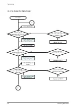
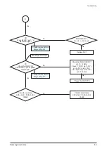
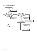
4-1-3 No Output (for Analog Input)
No output
1
Check if signal is measured
at pin 9 of ADIC1 of the
Main PCB.
Yes
2
Check the CLK at pin 10 of
ADIC1 of the Main PCB.
3
Check ADIC1 pin 1, 2
out / in signal.
Check the power(5V) pin 6 of
ADIC1 on the Main PCB
No
Yes
No
Check ADC Output.
A
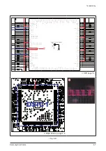
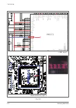
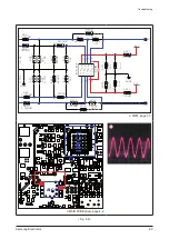
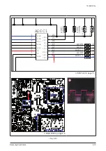
Refer to wave pattern
image of Fig. 4-9.
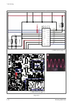
Refer to wave pattern
image of Fig. 4-10.
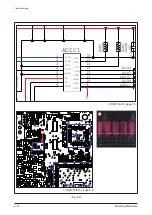
Refer to wave pattern
image of Fig. 4-8.
Yes
No
No
Replace the ADIC1
Summary of Contents for HW-C450
Page 16: ...3 4 Samsung Electronics MEMO ...
Page 35: ...Samsung Electronics 4 19 MEMO ...
Page 50: ...6 2 Samsung Electronics PCB Diagram 6 2 VFD PCB Top CN1 ...
Page 51: ...Samsung Electronics 6 3 PCB Diagram 6 3 VFD PCB Bottom ...
Page 52: ...6 4 Samsung Electronics PCB Diagram 6 4 KEY PCB Top ...
Page 53: ...Samsung Electronics 6 5 PCB Diagram 6 5 KEY PCB Bottom IC1 ...
Page 57: ...Samsung Electronics 6 9 PCB Diagram 6 7 MAIN PCB Bottom TP3 TP5 DIIC1 DSIC3 PWIC1 IC1 ...
Page 58: ...6 10 Samsung Electronics PCB Diagram 6 7 1 Test Point Wave Form TP3 TP5 ...
Page 59: ...Samsung Electronics 6 11 PCB Diagram 6 8 SMPS PCB Top 1 CN2 CN1 ...
Page 61: ...Samsung Electronics 6 13 PCB Diagram 6 9 SMPS PCB Bottom ...
Page 62: ...6 14 Samsung Electronics MEMO ...
Page 72: ...7 10 Samsung Electronics MEMO ...

