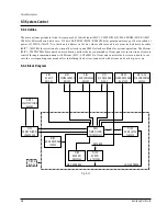
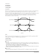
Circuit Descriptions
5-14
Samsung Electronics
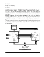
5-5 DVD Data Processor
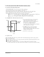
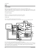
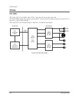
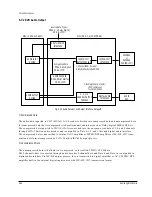
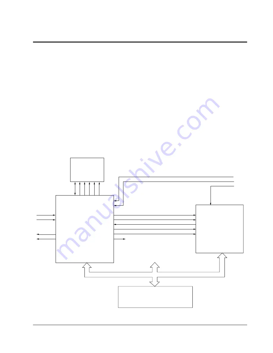
5-5-1 Outline
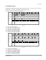
DIC1(KS1453) performs Sync detection, EFM/EFM demodulation and error correction and Spindle motor control
(CLV control) after inputting sliced EFM signal of RF signal at disc playback and EFM read clock (PLCK) signal gen-
erated from PLL. Outputs data which converted to the last audio and video from A/V decoder(VIC1). KS1453 uses
external memory(4M DRAM) as buffer as well as for error correction and carries out Variable Bit Rate transfer func-
tion. VBR function uses the external buffer as buffer to absorb the difference of transfer rate occurring because the
transfer rate of disc playback is faster than data transfer rate demanded by A/V decoder(Video/Audio Signal
Process Chip).
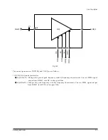
In case of general disc refresh, the memory is almost filled up periodically. It is because Write rate to memory after
disc playback and signal process is faster than Read of A/V decoder. When the memory is filled, this status is report-
ed by interrupt to main micom, which controls the servo to kick back the pick-up to the previous track after mem-
orizing the last data read from disc until now. It takes some times to jump to the previous track and return to the
original(jump location) again. The memory will have an empty space because A/V decoder reads out data of mem-
ory.
When the memory has an empty space, where data can be processed and written and the pick-up correctly gets to
the original location(before kick back location) again, it reads data again avoids the interrupt of data read previ-
ously. The basic operation repeats to perform as described above.
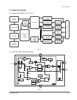
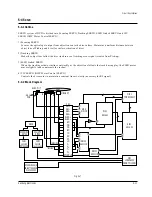
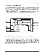
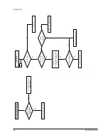
5-5-2 Block Diagram
Fig. 5-19
AD[7..0]
HA[23..8]
*WR(73)
INTO(ZIRQZD)
INT4(/INT)
*RD(72)
MIC1 TMP93CM41F
HDATA[7..0]
HADDR[3..0]
/CS
/RD
/WR
/INT
DVD-D[7..0]
VSTROBE
REQUEST
DACK
*ERR
VIC1
(ZiVA-3)
192
191
196
200
177, 178
CLOCK 27MHz
CLOCK 33.8688MHz
CLOCK 27MHz
14
95
69
70
58
71
57
SDATA[7..0]
CSTROBE
DATREQ
DATACK
DTER
TOS
O
E
W
E
C
A
S
R
A
S
[
[D
1
5.
.
0
[
[A
8.
.
0
[
[
D
D
1
5.
.
0
[
[
D
A
D
R
8.
.
0
Z
R
A
S
Z
C
A
S
Z
W
E
O
Z
O
E
O
MDAT[7:0]
MRZA(3)
ZCS(2)
MWR(128)
MRD(127)
ZIRQZD(126)
EFMI
PLCK
116
104
109
110
MDP
MDS
EFM
PLCK
DIC1
(KS1453)
DIC2
(KM416C254)
Summary of Contents for DVD-C700
Page 23: ...Reference Information 2 16 Samsung Electronics MEMO ...
Page 49: ...4 24 Samsung Electronics Disassembly and Reaasembly MEMO ...
Page 83: ...Troubleshooting 6 14 Samsung Electronics MEMO ...
Page 89: ...Exploded Views and Parts List 7 6 Samsung Electronics MEMO ...
Page 101: ...8 12 Samsung Electronics Electrical Parts List MEMO ...
Page 105: ...PCB Diagrams 10 2 Samsung Electronics 10 1 Main COMPONENT SIDE SOLDER SIDE ...
Page 106: ...PCB Diagrams Samsung Electronics 10 3 10 2 Jack ...
Page 107: ...PCB Diagrams 10 4 Samsung Electronics 10 3 S M P S ...
Page 108: ...PCB Diagrams Samsung Electronics 10 5 10 4 Front COMPONENT SIDE SOLDER SIDE ...
Page 109: ...PCB Diagrams 10 6 Samsung Electronics 10 5 Key COMPONENT SIDE SOLDER SIDE ...
Page 110: ...PCB Diagrams Samsung Electronics 10 7 10 6 Head Phone 10 7 Deck COMPONENT SIDE SOLDER SIDE ...
Page 111: ...PCB Diagrams 10 8 Samsung Electronics 10 8 Sensor 10 9 Motor ...
Page 113: ...Wiring Diagram 11 2 Samsung Electronics MEMO ...
Page 115: ...Schematic Diagrams 12 2 Samsung Electronics 12 1 S M P S ...
Page 116: ...Schematic Diagrams Samsung Electronics 12 3 12 2 Main Power Supply ...
Page 117: ...Schematic Diagrams 12 4 Samsung Electronics 12 3 Main Micom ...
Page 118: ...Schematic Diagrams Samsung Electronics 12 5 12 4 Servo ...
Page 119: ...Schematic Diagrams 12 6 Samsung Electronics 12 5 Video Encoder ...
Page 120: ...Schematic Diagrams Samsung Electronics 12 7 12 6 Video CVBS Output Y Output C Output ...
Page 121: ...Schematic Diagrams 12 8 Samsung Electronics 12 7 Audio DAC ...
Page 122: ...Schematic Diagrams Samsung Electronics 12 9 12 8 Audio ...
Page 123: ...Schematic Diagrams 12 10 Samsung Electronics 12 9 RF ...
Page 124: ...Schematic Diagrams Samsung Electronics 12 11 12 10 ZiVA ...
Page 125: ...Schematic Diagrams 12 12 Samsung Electronics 12 11 DSP ...
Page 126: ...Schematic Diagrams Samsung Electronics 12 13 12 12 Front Micom VFD Display ...
Page 128: ...Schematic Diagrams Samsung Electronics 12 15 12 14 Head Phone ...
Page 129: ...Schematic Diagrams 12 16 Samsung Electronics 12 15 Key ...
Page 130: ...Schematic Diagrams Samsung Electronics 12 17 12 16 Deck ...
Page 131: ...Schematic Diagrams 12 18 Samsung Electronics 12 17 Deck Control ...
Page 132: ...Schematic Diagrams Samsung Electronics 12 19 12 18 Remote Control ...
Page 133: ...Schematic Diagrams 12 20 Samsung Electronics MEMO ...