
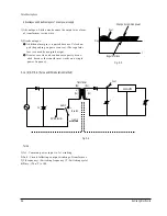
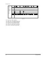
Circuit Descriptions
Samsung Electronics
5-3
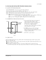
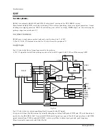
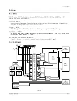
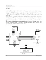
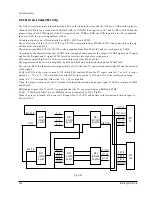
5-1-2 Circuit description (FLY-Back PWM (Plise Width Modulation) Control)
5-1-2 (a) AC Power Rectification/Smoothing Terminal
1) PD01,PD02,PD03,PD04 : Convert AC power to DC(Wave rectification)
2) PE3 : Smooth the voltage converted to DC(Refer to VIN of Fig. 5-7)
3) PC01, PC02, PC10, PC11, PC12, PC13, PL01, PL02, PL03 : Noise removal at power input/output
4) PVA1 : SMPS protection at power surge input (PVA1 pattern open is to remove noise)
5) PR10 : Rush current limit resistance at the moment of power cord insertion.
Œ
Rush current = (AC input voltage x 1.414 - Diode drop voltage) / Pattern resi PL02,01 resis-
tance + PC10 resi PR10) (AC230V based : approx. 26A)
´
Without PR10, the bridge diode might be damaged as the rush current increases.
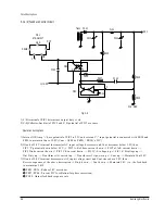
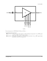
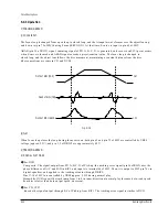
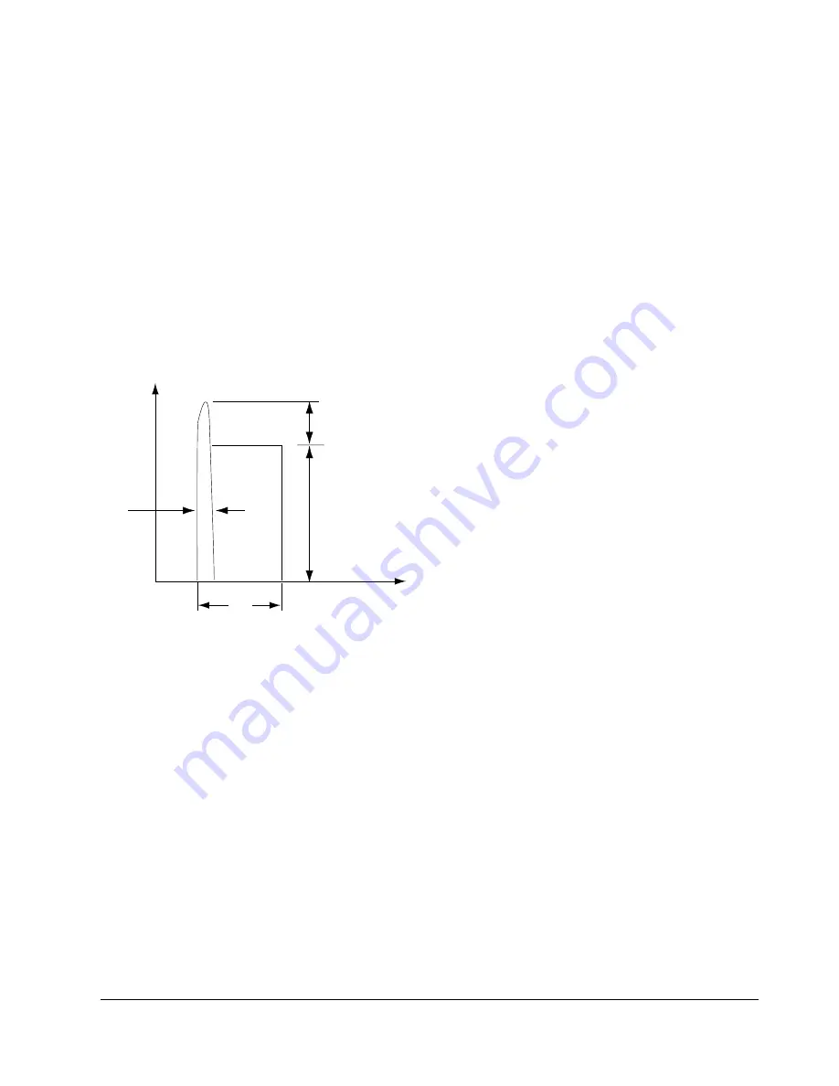
5-1-2 (b) SNUBBER Circuit : PR15, PR16, PC04, PC05, PD11, PR17
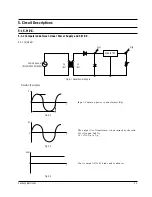
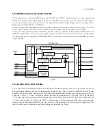
0
Vswitch
dt
Toff
t
Inverted power
by leakage
inductance
Fig. 5-7
1) Prevent residual high voltage at the terminals of
switch during switch off/Suppress noise.
High inverted power occurs at switch (PIC1) off,
because of the 1st winding of transformer :
(V= LI xdi/dt. LI : Leakage Induction)
A very high residual voltage exists on both terminals
of PIC1 because dt is a very short.
2) SNUBBER circuit protects PIC1 from damage
through leakage voltage suppression by RC,
(Charges the leakage voltage to PD11 and PC04, and
discharges to PR15 and PR16).
3) PC05, PR17 : For noise removal
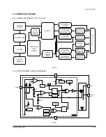
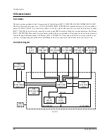
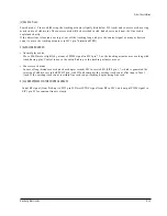
5-1-2 (c) PIC1 Vcc circuit
1) PR11, PR12, PR13, PR14 : PIC1 driving resistance (PIC1 works through driving resistance at power cord in)
2) PIC1 Vcc : PR18, PD12, PE6
Œ
Use the output of transformer as Vcc, because the current starts to flow into transformer while PIC1 is active.
´
Rectify to PD12 and smooth to PE6.
ˇ
Use the output of transformer as PIC1 Vcc : The loads are different before and after PIC1 driving.
(Vcc of PIC1 decreases below OFF voltage, using only the resistance due to load increase after PIC1 driving.)
Summary of Contents for DVD-C700
Page 23: ...Reference Information 2 16 Samsung Electronics MEMO ...
Page 49: ...4 24 Samsung Electronics Disassembly and Reaasembly MEMO ...
Page 83: ...Troubleshooting 6 14 Samsung Electronics MEMO ...
Page 89: ...Exploded Views and Parts List 7 6 Samsung Electronics MEMO ...
Page 101: ...8 12 Samsung Electronics Electrical Parts List MEMO ...
Page 105: ...PCB Diagrams 10 2 Samsung Electronics 10 1 Main COMPONENT SIDE SOLDER SIDE ...
Page 106: ...PCB Diagrams Samsung Electronics 10 3 10 2 Jack ...
Page 107: ...PCB Diagrams 10 4 Samsung Electronics 10 3 S M P S ...
Page 108: ...PCB Diagrams Samsung Electronics 10 5 10 4 Front COMPONENT SIDE SOLDER SIDE ...
Page 109: ...PCB Diagrams 10 6 Samsung Electronics 10 5 Key COMPONENT SIDE SOLDER SIDE ...
Page 110: ...PCB Diagrams Samsung Electronics 10 7 10 6 Head Phone 10 7 Deck COMPONENT SIDE SOLDER SIDE ...
Page 111: ...PCB Diagrams 10 8 Samsung Electronics 10 8 Sensor 10 9 Motor ...
Page 113: ...Wiring Diagram 11 2 Samsung Electronics MEMO ...
Page 115: ...Schematic Diagrams 12 2 Samsung Electronics 12 1 S M P S ...
Page 116: ...Schematic Diagrams Samsung Electronics 12 3 12 2 Main Power Supply ...
Page 117: ...Schematic Diagrams 12 4 Samsung Electronics 12 3 Main Micom ...
Page 118: ...Schematic Diagrams Samsung Electronics 12 5 12 4 Servo ...
Page 119: ...Schematic Diagrams 12 6 Samsung Electronics 12 5 Video Encoder ...
Page 120: ...Schematic Diagrams Samsung Electronics 12 7 12 6 Video CVBS Output Y Output C Output ...
Page 121: ...Schematic Diagrams 12 8 Samsung Electronics 12 7 Audio DAC ...
Page 122: ...Schematic Diagrams Samsung Electronics 12 9 12 8 Audio ...
Page 123: ...Schematic Diagrams 12 10 Samsung Electronics 12 9 RF ...
Page 124: ...Schematic Diagrams Samsung Electronics 12 11 12 10 ZiVA ...
Page 125: ...Schematic Diagrams 12 12 Samsung Electronics 12 11 DSP ...
Page 126: ...Schematic Diagrams Samsung Electronics 12 13 12 12 Front Micom VFD Display ...
Page 128: ...Schematic Diagrams Samsung Electronics 12 15 12 14 Head Phone ...
Page 129: ...Schematic Diagrams 12 16 Samsung Electronics 12 15 Key ...
Page 130: ...Schematic Diagrams Samsung Electronics 12 17 12 16 Deck ...
Page 131: ...Schematic Diagrams 12 18 Samsung Electronics 12 17 Deck Control ...
Page 132: ...Schematic Diagrams Samsung Electronics 12 19 12 18 Remote Control ...
Page 133: ...Schematic Diagrams 12 20 Samsung Electronics MEMO ...