
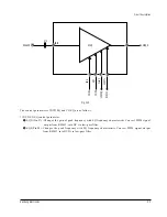
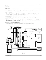
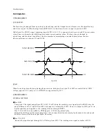
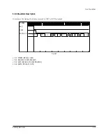
Circuit Descriptions
5-8
Samsung Electronics
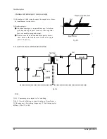
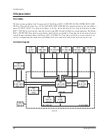
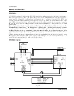
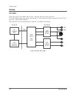
5-3 System Control
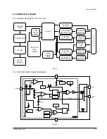
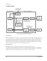
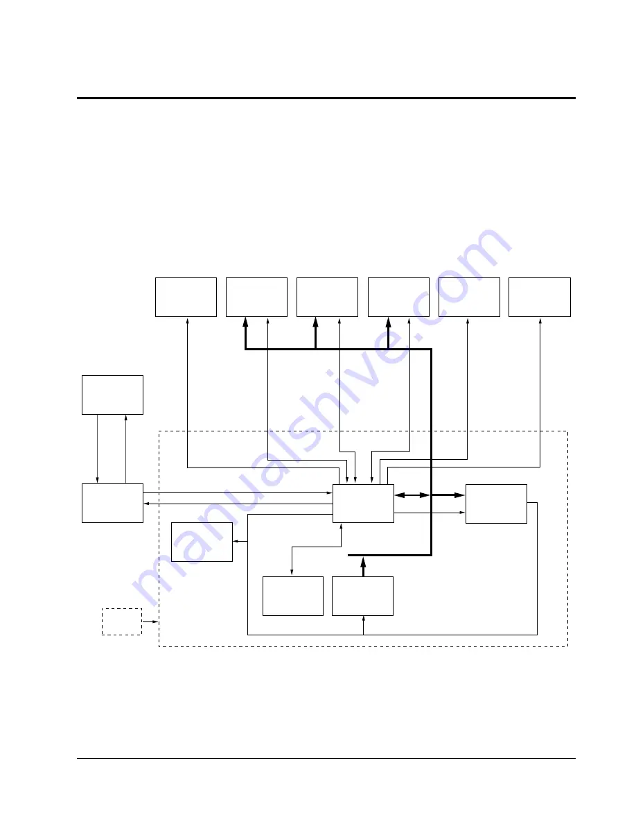
5-3-1 Outline
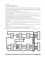
The main micom peripheral circuit is composed of 16bit Micom (MIC1 ; TMP93CM41F), 8M EPROM (MIC8 ; AM27-
C080) for Microcode and data save, 512 byte EE-PROM (MIC5 ; KS24C020) for permanent storage of data needed at
power off, MIC4 (74AC573) to latch only address in the bus where address and data are mixed, address decoder
(MIC7 ; 74HC00) for selection of ex-ternal device chip and 20MHz clock oscillator for micom operation. The Micom
(MIC1 ; TMP93CM41F) mounted in main board analizes the key commands of front panel or instructions of remote
control through communication with Micom (FIC1 ; LC86P6232) of front and controls the devices on board to exe-
cute the corresponding commands after initializing the devices connected with micom on board at power on.
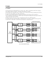
5-3-2 Block Diagram
RIC1
RF AMP
KS1461
SIC1
DIGITAL SERVO
KS1452
VIC1
A/V DECODER
ZIVA-3
VIC50
VIDEO ENCODER
SAA7128
AIC1,2,3,4
D/A CONVERTER
AK4324
DIC1
DATA PROCESSOR
KS1453
MIC2
ADDR LATCH
74AC573
MIC1
MAIN MICOM
TMP93CM41F
MIC8
EPROM
AT27C080
MIC5
EEPROM
KS24C020
MICOM
BLOCK
HIGH ADDRESS
LOW ADDRESS
DATA BUS
FIC1
FRONT MICOM
LC86P6232
DRIC3
ROULETTE MOTOR DRIVE
Ka3082
MIC7
ADDR DECODER
74HC00
Fig. 5-13
Summary of Contents for DVD-C700
Page 23: ...Reference Information 2 16 Samsung Electronics MEMO ...
Page 49: ...4 24 Samsung Electronics Disassembly and Reaasembly MEMO ...
Page 83: ...Troubleshooting 6 14 Samsung Electronics MEMO ...
Page 89: ...Exploded Views and Parts List 7 6 Samsung Electronics MEMO ...
Page 101: ...8 12 Samsung Electronics Electrical Parts List MEMO ...
Page 105: ...PCB Diagrams 10 2 Samsung Electronics 10 1 Main COMPONENT SIDE SOLDER SIDE ...
Page 106: ...PCB Diagrams Samsung Electronics 10 3 10 2 Jack ...
Page 107: ...PCB Diagrams 10 4 Samsung Electronics 10 3 S M P S ...
Page 108: ...PCB Diagrams Samsung Electronics 10 5 10 4 Front COMPONENT SIDE SOLDER SIDE ...
Page 109: ...PCB Diagrams 10 6 Samsung Electronics 10 5 Key COMPONENT SIDE SOLDER SIDE ...
Page 110: ...PCB Diagrams Samsung Electronics 10 7 10 6 Head Phone 10 7 Deck COMPONENT SIDE SOLDER SIDE ...
Page 111: ...PCB Diagrams 10 8 Samsung Electronics 10 8 Sensor 10 9 Motor ...
Page 113: ...Wiring Diagram 11 2 Samsung Electronics MEMO ...
Page 115: ...Schematic Diagrams 12 2 Samsung Electronics 12 1 S M P S ...
Page 116: ...Schematic Diagrams Samsung Electronics 12 3 12 2 Main Power Supply ...
Page 117: ...Schematic Diagrams 12 4 Samsung Electronics 12 3 Main Micom ...
Page 118: ...Schematic Diagrams Samsung Electronics 12 5 12 4 Servo ...
Page 119: ...Schematic Diagrams 12 6 Samsung Electronics 12 5 Video Encoder ...
Page 120: ...Schematic Diagrams Samsung Electronics 12 7 12 6 Video CVBS Output Y Output C Output ...
Page 121: ...Schematic Diagrams 12 8 Samsung Electronics 12 7 Audio DAC ...
Page 122: ...Schematic Diagrams Samsung Electronics 12 9 12 8 Audio ...
Page 123: ...Schematic Diagrams 12 10 Samsung Electronics 12 9 RF ...
Page 124: ...Schematic Diagrams Samsung Electronics 12 11 12 10 ZiVA ...
Page 125: ...Schematic Diagrams 12 12 Samsung Electronics 12 11 DSP ...
Page 126: ...Schematic Diagrams Samsung Electronics 12 13 12 12 Front Micom VFD Display ...
Page 128: ...Schematic Diagrams Samsung Electronics 12 15 12 14 Head Phone ...
Page 129: ...Schematic Diagrams 12 16 Samsung Electronics 12 15 Key ...
Page 130: ...Schematic Diagrams Samsung Electronics 12 17 12 16 Deck ...
Page 131: ...Schematic Diagrams 12 18 Samsung Electronics 12 17 Deck Control ...
Page 132: ...Schematic Diagrams Samsung Electronics 12 19 12 18 Remote Control ...
Page 133: ...Schematic Diagrams 12 20 Samsung Electronics MEMO ...