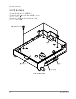
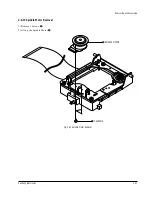
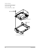
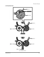
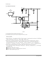
Circuit Descriptions
5-6
Samsung Electronics
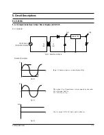
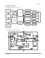
5-2 RF
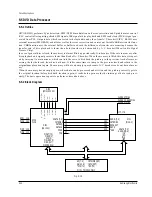
5-2-1 RIC1 (KS1461)
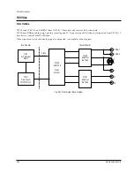
KS1461 is combined with KS1452 and KS1453 as bipolar IC developed for DVD SERVO system.
Main features include DVD waveform equalizing, CD waveform equalizing, focus error signal generation, 3-beam
tracking error signal generation, DPD 1-beam tracking error, defect, envelope, MIRR output, etc. after receiving the
pick-up output converted into I/V.
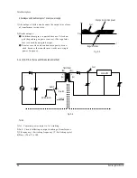
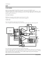
5-2-1 (a) Basic Potentiometer
KS1461 uses a single power method and each circuit is based on V of 2.5V.
V (Pin 12, 20, 24, 67) terminal is needed for IC, which uses the peripheral V.
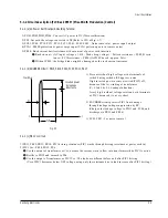
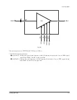
5-2-1(b) RF signal
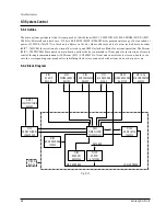
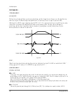
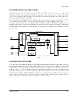
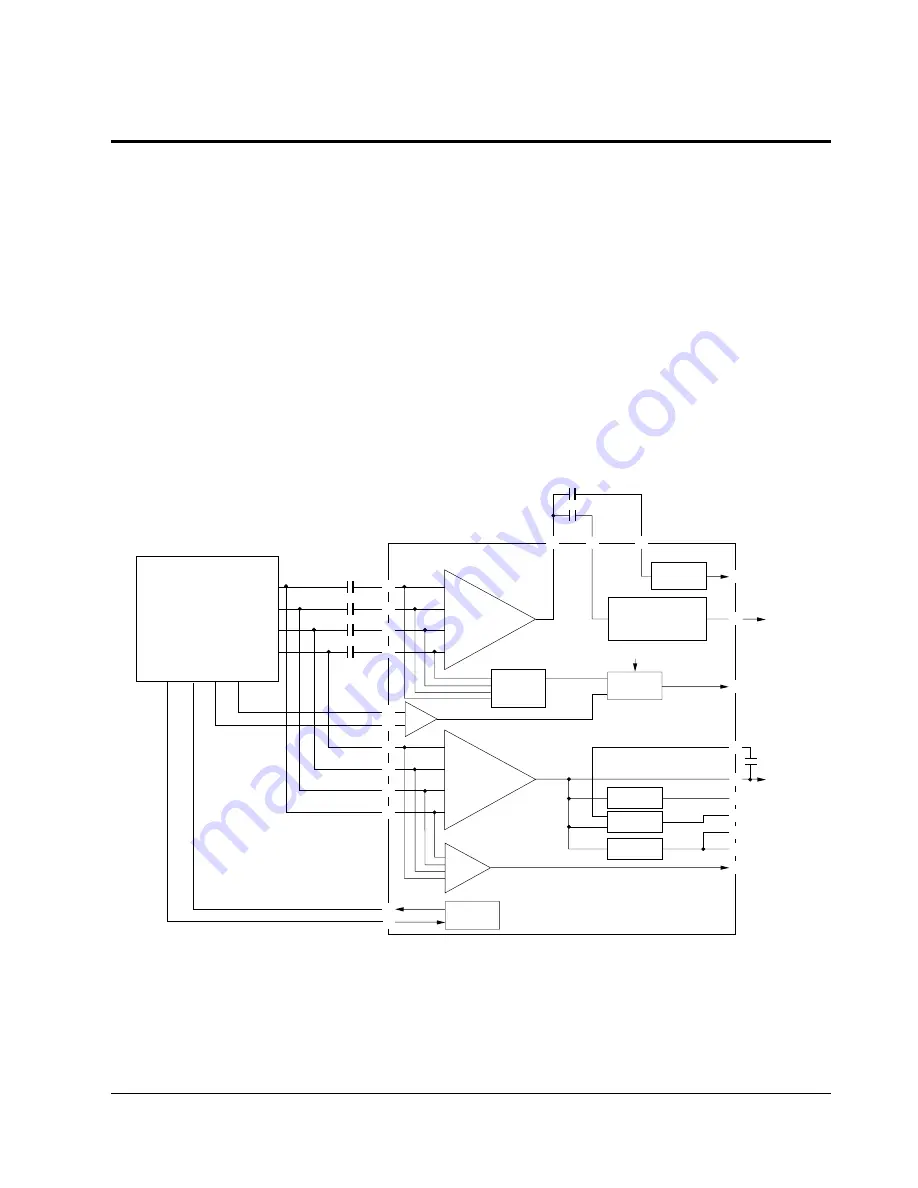
Fig. 5-11 shows the flow of signal generated by the pick-up.
A, B, C, D signals detected from pick-up are converted in to RF signal(A+B+C+D) via RF summing AMP.
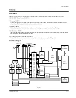
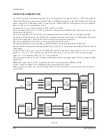
Fig. 5-12 shows the waveform-equalizing block diagram for the RF signal.
It outputs to EQout (Pin 86) terminal by initially changing switching AMP gain of DVD and CD, and then adjust-
ing the level in RF SUM & AGC. It controls RF SUM & AGC gain by means of Pin 89-95 and interfaces with PWM
signal, (output from PWM terminal of KS1453, via low-pass filter to adjust boost gain and peak frequency.
EQout terminal is connected with EQin (Pin 86).
PICK-UP
RE SUM
& AGC
RF EG
DPD
TE
Mhx
ENV
FOK
DEFECT
TESEL
TE
ABCD
SUM
FE
ALPC
MIRR
%
^
&
*
5
6
7
8
3
4
104
104
104
104
?
.
m
474
104
RFAGCO
EQIN
MIRRI
G
,
y
I
i
T
F
P
[
d
MIRR
TE
RFEQO
A
B
C
D
E
F
LD
PD
w
E
ABCD
FE
DFCT1
DFCT2
FOKB
ENV
103
ABCDI
Fig. 5-11
Summary of Contents for DVD-C700
Page 23: ...Reference Information 2 16 Samsung Electronics MEMO ...
Page 49: ...4 24 Samsung Electronics Disassembly and Reaasembly MEMO ...
Page 83: ...Troubleshooting 6 14 Samsung Electronics MEMO ...
Page 89: ...Exploded Views and Parts List 7 6 Samsung Electronics MEMO ...
Page 101: ...8 12 Samsung Electronics Electrical Parts List MEMO ...
Page 105: ...PCB Diagrams 10 2 Samsung Electronics 10 1 Main COMPONENT SIDE SOLDER SIDE ...
Page 106: ...PCB Diagrams Samsung Electronics 10 3 10 2 Jack ...
Page 107: ...PCB Diagrams 10 4 Samsung Electronics 10 3 S M P S ...
Page 108: ...PCB Diagrams Samsung Electronics 10 5 10 4 Front COMPONENT SIDE SOLDER SIDE ...
Page 109: ...PCB Diagrams 10 6 Samsung Electronics 10 5 Key COMPONENT SIDE SOLDER SIDE ...
Page 110: ...PCB Diagrams Samsung Electronics 10 7 10 6 Head Phone 10 7 Deck COMPONENT SIDE SOLDER SIDE ...
Page 111: ...PCB Diagrams 10 8 Samsung Electronics 10 8 Sensor 10 9 Motor ...
Page 113: ...Wiring Diagram 11 2 Samsung Electronics MEMO ...
Page 115: ...Schematic Diagrams 12 2 Samsung Electronics 12 1 S M P S ...
Page 116: ...Schematic Diagrams Samsung Electronics 12 3 12 2 Main Power Supply ...
Page 117: ...Schematic Diagrams 12 4 Samsung Electronics 12 3 Main Micom ...
Page 118: ...Schematic Diagrams Samsung Electronics 12 5 12 4 Servo ...
Page 119: ...Schematic Diagrams 12 6 Samsung Electronics 12 5 Video Encoder ...
Page 120: ...Schematic Diagrams Samsung Electronics 12 7 12 6 Video CVBS Output Y Output C Output ...
Page 121: ...Schematic Diagrams 12 8 Samsung Electronics 12 7 Audio DAC ...
Page 122: ...Schematic Diagrams Samsung Electronics 12 9 12 8 Audio ...
Page 123: ...Schematic Diagrams 12 10 Samsung Electronics 12 9 RF ...
Page 124: ...Schematic Diagrams Samsung Electronics 12 11 12 10 ZiVA ...
Page 125: ...Schematic Diagrams 12 12 Samsung Electronics 12 11 DSP ...
Page 126: ...Schematic Diagrams Samsung Electronics 12 13 12 12 Front Micom VFD Display ...
Page 128: ...Schematic Diagrams Samsung Electronics 12 15 12 14 Head Phone ...
Page 129: ...Schematic Diagrams 12 16 Samsung Electronics 12 15 Key ...
Page 130: ...Schematic Diagrams Samsung Electronics 12 17 12 16 Deck ...
Page 131: ...Schematic Diagrams 12 18 Samsung Electronics 12 17 Deck Control ...
Page 132: ...Schematic Diagrams Samsung Electronics 12 19 12 18 Remote Control ...
Page 133: ...Schematic Diagrams 12 20 Samsung Electronics MEMO ...