


LPWA Module Series
BG95 Hardware Design
BG95_Hardware_Design 51 / 80
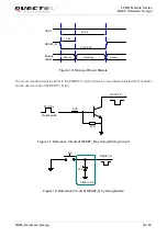
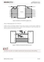
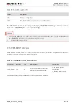
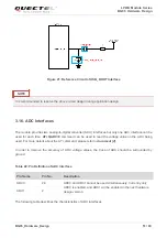
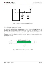
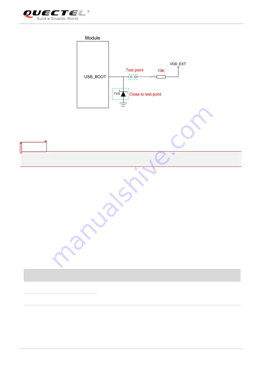
Figure 21: Reference Circuit of USB_BOOT Interface
It is recommended to reserve the above circuit design during application design.
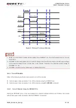
3.16. ADC Interfaces
The module provides two analog-to-digital converter (ADC) interfaces but only one ADC interface can be
used for each time.
AT+QADC=0
command can be used to read the voltage value on the ADC being
used. For more details about the AT command, please refer to
document [2]
.
In order to improve the accuracy of ADC voltage values, the trace of ADC should be surrounded by
ground.
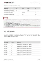
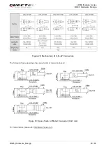
Table 22: Pin Definition of ADC Interface
The following table describes the characteristics of ADC interfaces.
Pin Name
Pin No.
Description
ADC0 24 ADC0 and ADC1 cannot be used simultaneously. Currently only
ADC0 is enabled, and ADC1 will be enabled in the next hardware
design version.
ADC1 2
NOTE


