

LPWA Module Series
BG95 Hardware Design
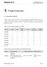
BG95_Hardware_Design 18 / 80
are also no effects on radio spectrum and no harm to radio network. Only one or more parameters like
P
out
might reduce in their value and exceed the specified tolerances. When the temperature returns to
the normal operating temperature levels, the module will meet 3GPP specifications again.
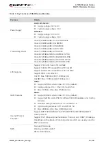
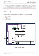
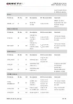
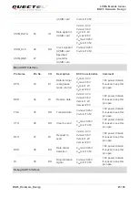
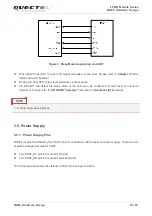
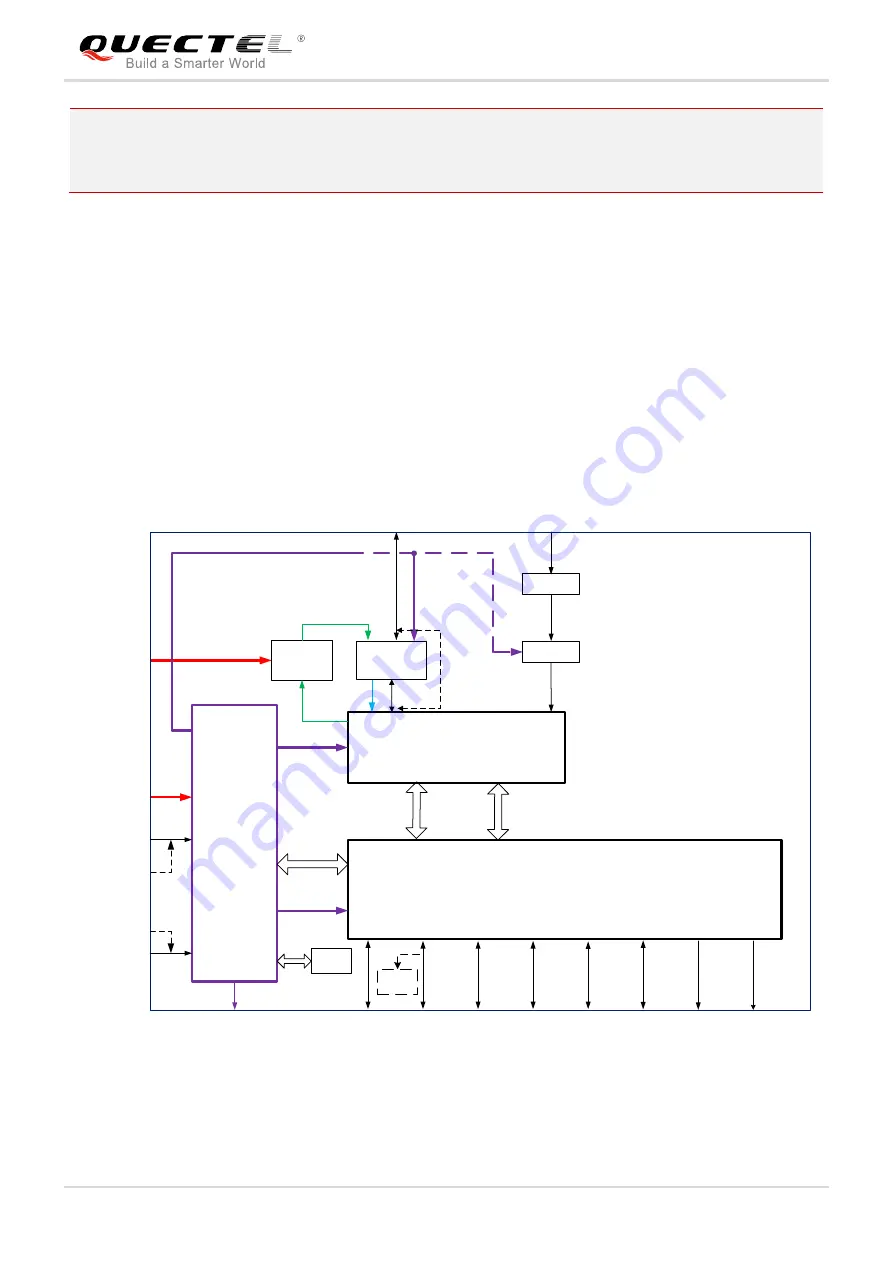
2.3. Functional Diagram
The following figure shows a block diagram of BG95 and illustrates the major functional parts.
Power
management
Baseband
Radio
frequency
Peripheral
interfaces
Baseband
PMIC
Transceiver/PA/switch
SAW
ANT_MAIN
ANT_GNSS
VBAT_BB
VBAT_RF
PWRKEY
VDD_EXT
USB
(U)SIM
PCM*
I2C*
19.2M
XO
GPIOs
Control
IQ
Control
LNA
Tx
Rx
GNSS
UARTs
PA
(GSM)
ADC0
(ASM)
STATUS NETLIGHT
eSIM
RESET_N
ADC1
Figure 1: Functional Diagram


