


LPWA Module Series
BG95 Hardware Design
BG95_Hardware_Design 29 / 80
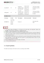
1.
1)
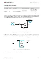
The output voltage of PWRKEY is 1.5V because of the diode drop in the Qualcomm chipset, and
PWRKEY should never be pulled down to GND permanently.
2.
2)
RESET_N will be supported in the next hardware design version.
3.
3)
ADC0 and ADC1 cannot be used simultaneously. BG95 supports using of only one ADC interface at
a time: either ADC0 or ADC1. Currently only ADC0 is enabled, and ADC1 will be enabled in the next
hardware design version.
4.
4)
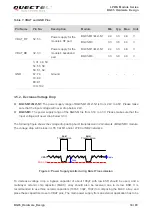
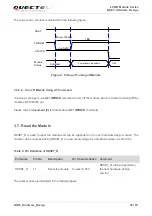
When PSM is enabled, the function of PSM_IND* pin will be activated after the module is rebooted.
When PSM_IND* is in high voltage level, the module is in normal operation state, when it is in low
voltage level, the module is in PSM.
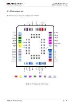
5. Keep all RESERVED pins and unused pins unconnected.
6. “*” means under development.
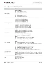
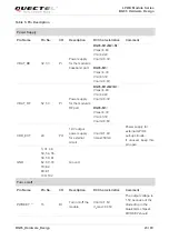
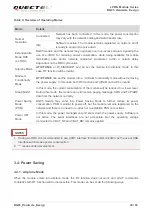
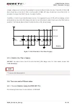
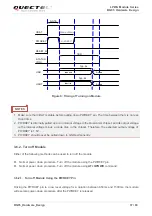
3.3. Operating Modes
The table below briefly summarizes the various operating modes of BG95.
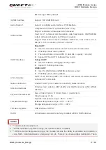
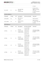
AP_READY* 19
DI
Application
processor sleep
state detection
V
IL
min=-0.3V
V
IL
max=0.6V
V
IH
min=1.2V
V
IH
max=2.0V
1.8V power domain.
If unused, keep this
pin open.
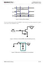
USB_BOOT 75
DI
Force the
module to enter
into emergency
download mode
V
IL
min=-0.3V
V
IL
max=0.6V
V
IH
min=1.2V
V
IH
max=2.0V
1.8V power domain.
If unused, keep this
pin open.
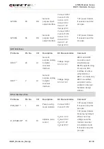
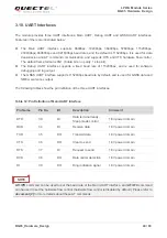
RESERVED Pins
Pin Name
Pin No.
I/O
Description
DC Characteristics
Comment
RESERVED
11~14, 51,
56, 57, 63,
76~78,
83~88,
92~99
Reserved
Keep these pins
open.
NOTES


