


LPWA Module Series
BG95 Hardware Design
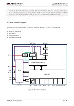
BG95_Hardware_Design 22 / 80
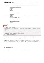
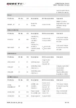
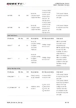
1.
1)
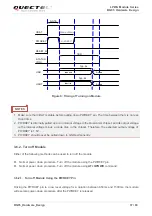
ADC0 and ADC1 cannot be used simultaneously. BG95 supports using of only one ADC interface
at a time: either ADC0 or ADC1. Currently only ADC0 is enabled, and ADC1 will be enabled in the
next hardware design version.
2.
2)
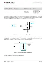
PWRKEY output voltage is 1.5V because of the diode drop in the Qualcomm chipset. PWRKEY
should never be pulled down to GND permanently.
3.
3)
RESET_N will be supported in the next hardware design version.
4. Keep all RESERVED pins and unused pins unconnected.
5. GND pins should be connected to ground in the design.
6. “*” means under development.
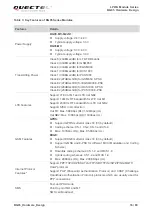
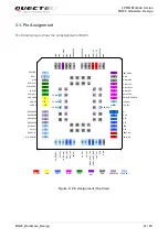
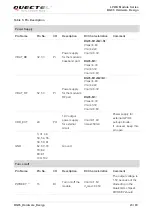
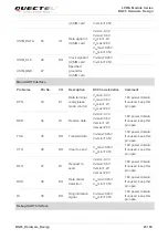
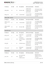
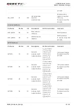
3.2. Pin Description
The following tables show the pin definition and description of BG95.
Table 4: Definition of I/O Parameters
Type
Description
AI Analog
Input
AO Analog
Output
DI Digital
Input
DO Digital
Output
IO Bidirectional
OD Open
Drain
PI Power
Input
PO Power
Output
NOTES


