LPWA Module Series
BG95&BG96 Compatible Design
BG95&BG96_Compatible_Design 20 / 47
1.
1)
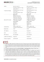
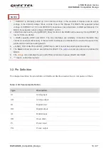
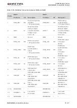
When PSM is enabled, the function of PSM_IND pin will be activated after the module is rebooted.
When PSM_IND is in high voltage level, the module is in normal operation state, and when it is in low
voltage level, the module is in PSM.
2.
2)
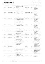
BG95 supports
ADC0 and ADC1. The two interfaces are internally connected, therefore they
cannot be used simultaneously. If the two ADC interfaces are intended to be used at the same time,
please add an external analog switch.
3.
3)
PWRKEY is internally pulled up to an internal voltage in the Qualcomm chipset, and its output
interface.
1.8V power
domain.
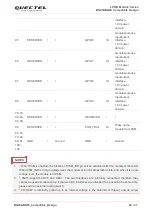
85
RESERVED
/
/
GPIO6
IO
General-purpose
input/output
interface.
1.8V power
domain.
86
RESERVED
/
/
GPIO7
IO
General-purpose
input/output
interface.
1.8V power
domain.
87
RESERVED
/
/
GPIO8
IO
General-purpose
input/output
interface.
1.8V power
domain.
88
RESERVED
/
/
GPIO9
IO
General-purpose
input/output
interface.
1.8V power
domain.
76~78,
92~95,
97~99
RESERVED
/
/
RESERVED
/
/
96
RESERVED
/
/
PON_TRIG
DI
Wake up the
module from PSM
67~74,
79~82,
89~91,
100~
102
GND
/
Ground
GND
/
Ground
NOTES


