LPWA Module Series
BG95&BG96 Compatible Design
BG95&BG96_Compatible_Design 23 / 47
Special attention should be paid to the power supply design for BG95/BG96:
If only LTE Cat M1 and Cat NB1 networks are intended to be used, it is recommended to select a
DC-DC chip or LDO chip with ultra-low leakage current and current output no less than 1.0A as the
power supply.
If LTE Cat M1, Cat NB1 and EGPRS networks are all intended to be used, the current output of
DC-DC chip or LDO chip cannot be lower than 2.0A and power supply chips with low leakage current
should be selected because the module needs more current when transmitting in 2G condition.
4.1.2. Reduce Voltage Drop
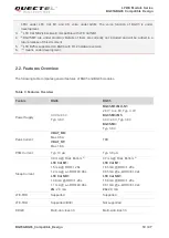
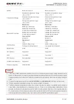
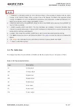
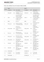
The power supply range of BG95 and BG96 modules are listed below:
BG96 and BG95-M3/-M5:
3.3V to 4.3V, typ. 3.8V
BG95-M1/-M2/-N1:
2.6V
to 4.8V, typ. 3.3V
BG95-M4:
typ. 3.8V
Please make sure the input voltage never drop below 3.3V or
exceed 4.2V in BG95 and BG96 compatible
design. The VBAT to BG95/BG96 module
’s VBAT_BB and VBAT_RF pins should be divided into two
separated paths in star structure.
In addition, in order to avoid the damage caused by electric surge and ESD, it is suggested that a TVS
diode with low reverse stand-off voltage (V
RWM
), low leakage current, low clamping voltage (V
C
) and high
reverse peak pulse current (I
PP
)
should be used.
The following figure shows a reference design of VBAT for BG95 and BG96.
Module
VBAT_RF
VBAT_BB
VBAT
C1
100uF
C6
100nF
C7
33pF
C8
10pF
+
+
C2
100nF
C5
100uF
C3
33pF
C4
10pF
D1
TVS
Figure 3: Reference Circuit of VBAT (BG95/BG96)


