LPWA Module Series
BG95&BG96 Compatible Design
BG95&BG96_Compatible_Design 21 / 47
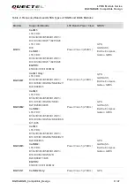
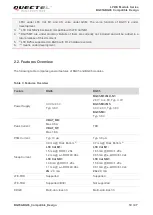
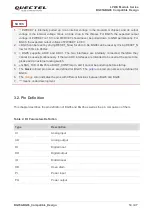
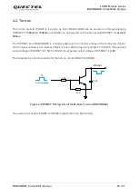
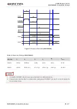
voltage is the internal voltage minus a diode drop in the chipset. For BG95, the expected output
voltage of PWRKEY is 1.5V, and PWRKEY should never be pulled down to GND permanently. For
BG96, the expected output voltage of PWRKEY is 0.8V.
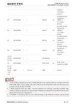
4.
4)
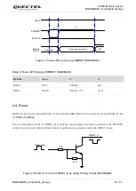
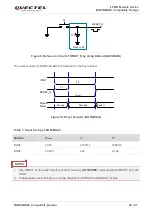
BG95 can be reset by driving RESET_N low for 2s to 3.8s. BG96 can be reset by driving RESET_N
low for 150ms to 460ms.
5.
5)
For every VBAT transition/re-insertion from 0V, the minimum power supply voltage should be more
than 2.7V. Meanwhile, in order to guaranteed stability and RF performance, the minimum power
supply voltage should be more than 2.8V. After the module startup normally, the minimum safety
voltage is 2.6V.
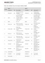
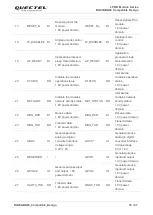
6. PSM_IND, W_DISABEL#, AP_READY, USIM_DET, PCM, I2C, GRFC and GPIO functions of BG95
are under development.
7. Keep all reserved and unused pins unconnected.
8. All GND pins should be connected to ground.
9.
“*” means under development.

