background image

Chapter 3 

36 

KEMF-4010 User’s 

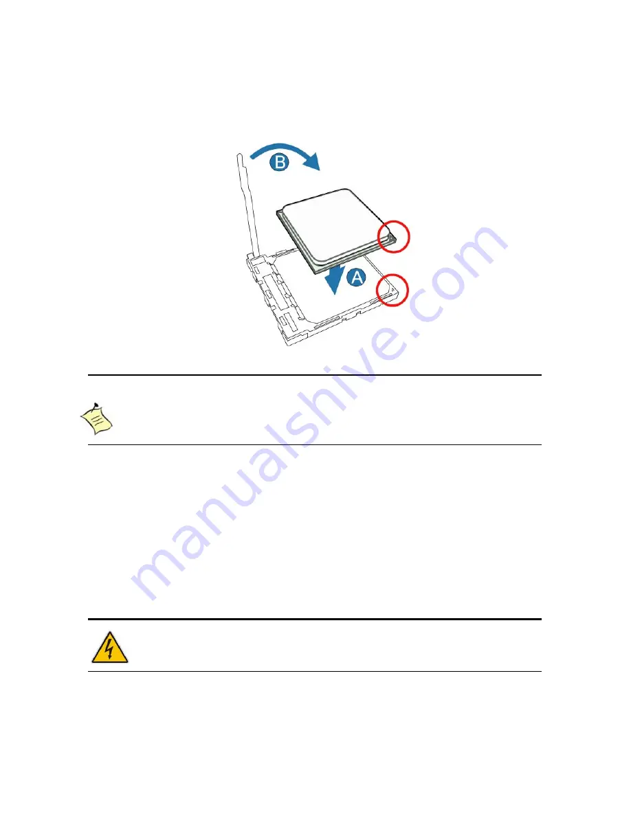
4.  Make sure that the CPU pins fit perfectly into their holes. Once the CPU is 

positioned into its socket, place one finger down on the middle of the CPU, lowering 
the locking lever and latching it into the fully locked position.   


Figure 6 CPU Installation 


NOTE  

You should not have to press down on the processor. If the processor does not drop 

completely into the socket, adjust the CPU orientation until the processor drops completely in. 


Removing the CPU: 

To remove the CPU, reverse the installation steps. 
1.  Before removing the CPU, turn off the system power and wait for about 20 minutes 

until the heat radiation plate of the cooling fan and the CPU cools down. 

2.  To remove the CPU, follow Step 2 of Installing the CPU above. 
3.  Remove the CPU by grasping the substrate edges only with thumb and forefinger 

and lifting it out with a purely vertical motion. 


WARNING 

The CPU and the heat-sink may be hot and could cause burns. 


Summary of Contents for KEMF-4010

Page 1: ...I KEMF 4010 User s KEMF 4010 FlexATX Embedded Motherboard with AMD Athlon Single and Dual Core Processors and AMD 780E SB710 chipset User s Guide...

Page 2: ...ed trademarks and trade names used in this user s guide are the property of their respective owners All rights reserved This user s guide contains information proprietary to Quanmax Customers may repr...

Page 3: ...pter 1 Introduction 14 Overview 14 Product Specifications 15 System Block Diagram 16 Mechanical Dimensions 17 Chapter 2 Hardware Settings 18 Overview 18 Jumper Settings and Pin Definitions 19 Jumper S...

Page 4: ...Setup 41 Overview 41 Main Menu 42 Advanced Menu 43 Boot Menu 48 Chipset Menu 48 Power Menu 50 Security Menu 51 Exit Menu 52 Chapter 5 Driver Installation 53 Appendix A DIO Digital I O Programming Guid...

Page 5: ...ons 19 Figure 5 CPU alignment in Socket AM2 35 Figure 6 CPU Installation 36 Figure 7 Place the CPU cooler on the retention frame 37 Figure 8 Hook the CPU cooler clip to the mounting lug 37 Figure 9 Lo...

Page 6: ...1 LAN2 LAN3 RJ 45 2 USB 2 0 Connector 23 Table 16 LAN LED Status 23 Table 17 PS2 KBMS1 PS 2 KB MS Mini DIN Connector 24 Table 18 HDMI1 HDMI Connector 24 Table 19 Internal Connector List 25 Table 20 AT...

Page 7: ...34 Table 42 BIOS Main Menu 42 Table 43 SATA and onboard CF Device Setting Menu 42 Table 44 System Information 43 Table 45 Advanced Menu 43 Table 46 CPU Feature 44 Table 47 OnBoard Peripherals Configu...

Page 8: ...guide for precautions and procedures If you have any questions please contact Quanmax Post Sales Technical Support WARNING High voltages are present inside the chassis when the unit s power cord is p...

Page 9: ...D workstation and follow proper ESD procedure to reduce the risk of damage to components Quanmax strongly encourages you to follow proper ESD procedure which can include wrist straps and smocks when s...

Page 10: ...Policy for the return procedure Regulatory Compliance Statements This section provides the FCC compliance statement for Class A devices FCC Compliance Statement for Class A Devices The product s descr...

Page 11: ...arty is authorized to change modify or extend the terms of this Limited Warranty in any manner whatsoever Quanmax reserves the right to make changes or improvements in any product without incurring an...

Page 12: ...for safe operation is not compromised Consideration should be given to the maximum rated ambient temperature Overheating can cause a variety of problems including premature aging and failure of chips...

Page 13: ...level Line Conditioner Line conditioners go beyond the over voltage protection of surge protectors Line conditioners keep a system s AC power source voltage at a fairly constant level and therefore c...

Page 14: ...HDMI 18 24 bit dual channel LVDS panel support SATA 3 Gb s RS 232 422 485 serial port DI DO Gigabit Ethernet USB 2 0 keyboard mouse and HD audio Mini PCIe PCIe x1 PCIe x16 and PCI support provides ex...

Page 15: ...pitch header for S PDIF Peripheral Support 1x CompactFlash socket 6x SATA 3Gb s RAID 0 1 10 support 10x USB 2 0 6x COMs with Power Selection 1x RS232 422 485 5x RS 232 1x IrDA support from remote cont...

Page 16: ...Chapter 1 16 KEMF 4010 User s System Block Diagram Figure 1 Block Diagram...

Page 17: ...Chapter 1 17 KEMF 4010 User s Mechanical Dimensions Figure 2 KEMF 4010 Mechanical Dimensions...

Page 18: ...gure 3 Jumper Connector For a three pin jumper see Figure 3 the jumper setting is designated 1 2 when the jumper connects pins 1 and 2 The jumper setting is designated 2 3 when pins 2 and 3 are connec...

Page 19: ...Chapter 2 19 KEMF 4010 User s Jumper Settings and Pin Definitions For jumper and connector locations please refer to the diagrams below Figure 4 KEMF 4010 Jumper and Connector Locations...

Page 20: ...ction JP11 Panel Power Selection JP12 Backlight Power Selection JP13 COM1 Signal Power Selection JP14 KB MS Signal Selection JP15 BL Signal Selection Table 3 JP1 JP2 JP3 JP6 JP7 JP13 COM Port Signal P...

Page 21: ...Open ATX mode Default Short AT mode Pitch 2 0mm YIMTEX 3291 02SAGR 6T Table 7 JP9 Clear CMOS Selection Jumper Status 1 2 Normal Operation Default 2 3 Clear CMOS Pitch 2 0mm YIMTEX 3291 03SAGR 6T Remar...

Page 22: ...Back Light Signal Selection Jumper Status 1 2 High Active Default 2 3 Low Active Pitch 2 0mm YIMTEX 3291 03SAGR 6T Rear Panel Pin Assignments Table 12 Rear Panel Connector List Label Function AUDIO1...

Page 23: ...a set ready C7 RTS Request to send C8 CTS Clear to send C9 RI Ring indicator C10 NC D201B1N01002N Note COM 1 RS 232 422 485 can be selected in BIOS setup Note RS 485 is half duplex mode Table 15 LAN1...

Page 24: ...12 NC No Connect MINI DIN DIP 6 6P MH11061 P36 4F 90D F FOXCONN Table 18 HDMI1 HDMI Connector Pin Signal 1 TMDS Data2 2 TMDS Data2 Shield 3 TMDS Data2 4 TMDS Data1 5 TMDS Data1 Shield 6 TMDS Data1 7 T...

Page 25: ...al ATA Connector HDMI_SPDIF1 SPD IF Output Pin Header SATAII_3 Serial ATA Connector CN1 Panel Backlight Wafer SATAII_4 Serial ATA Connector AMP_L1 Left Channel 2W Audio AMP Output Wafer SATAII_5 Seria...

Page 26: ...t 3 GND 8 33 GND GND 9 34 IDEIOR GND 10 35 IDEIOW GND 11 36 5V GND 12 37 IDEIRQ 5V 13 38 5V GND 14 39 PCSEL GND 15 40 NC GND 16 41 Reset IDE GND 17 42 IDEIORDY SDA2 18 43 DREQ IDE Address 1 19 44 DACK...

Page 27: ...Signal Name 1 5V 2 GND 3 SPD IF Output 4 GND Pitch 2 54mm YIMTEX 3321 04SAGR 6T Table 26 CN1 Panel Backlight Wafer Pin Signal Name 1 BL_EN 2 GND 3 5V 12V 4 5V 12V 5 GND 6 BL_ADJ 7 NC Pitch 1 25mm WAF...

Page 28: ...X 521AW1 03STR Table 31 FP1 Front Panel 1 Pin Header Pin Signal Pin Signal 1 Reset Button 2 Speaker 3 Reset Button 4 NC 5 HDD LED 6 Internal Speaker 7 HDD LED 8 Speaker Pitch 2 54mm YIMTEX 3322 04SAGR...

Page 29: ...29 I2C_Data Pitch 1 25mm Tin Plated HIROSE DF13 30DP 1 25 24 Cable 0C5029003000070L LVDS Port cable 30 pin 1 25mm to DVI connector with bracket L 30cm The voltage is selected by JP11 Note If DVI cabl...

Page 30: ...nd 31 3 3V AD 18 32 AD 17 AD 16 33 C BE 2 3 3V 34 Ground FRAME 35 IRDY Ground 36 3 3V TRDY 37 DEVSEL Ground 38 Ground STOP 39 LOCK 3 3V 40 PERR SMB_CLK 41 3 3V SMB_DAT 42 SERR Ground 43 3 3V PAR 44 C...

Page 31: ...Ground 24 HSON2 Ground 25 Ground HSIP2 26 Ground HSIP2 27 HSOP3 Ground 28 HSON3 Ground 29 Ground HSIP3 30 Reserved HSIP3 31 PRSNT 2 Ground 32 Ground Reserved 33 HSOP4 Reserved 34 HSON4 Ground 35 Groun...

Page 32: ...me 1 5V 2 5V 3 USB_A 4 USB_B 5 USB_A 6 USB_B 7 GND 8 GND 9 KEY 10 GND Pitch 2 54mm YIMTEX 3322 05SAGR 6T 09 Cable 0C502USB0201010L USB cable 2 54mm 10 pin to 2xUSB connectors with bracket L 30cm Table...

Page 33: ...le 40 SATAII_1 SATAII_2 SATAII_3 SATAII_4 SATAII_5 SATAII_6 Serial ATA Connector Pin Signal Name 1 GND 2 TX 3 TX 4 GND 5 RX 6 RX 7 GND FOXCONN LD1807V S52U Cable 0C501ATA0746000L SATA cable 7 pin conn...

Page 34: ...Ground 15 16 UIM_VPP Reserved 17 18 Ground Reserved 19 20 W_disable Ground 21 22 PERST PERn0 23 24 3VSB PERp0 25 26 Ground Ground 27 28 1 5V Ground 29 30 SMB_CLK PETn0 31 32 SMB_DATA PETp0 33 34 Grou...

Page 35: ...the substrate edges only with thumb and forefinger CAUTION Do not touch processor contacts to prevent damaging the CPU Installing the CPU Carefully follow the steps below in order to install the CPU 1...

Page 36: ...mpletely into the socket adjust the CPU orientation until the processor drops completely in Removing the CPU To remove the CPU reverse the installation steps 1 Before removing the CPU turn off the sys...

Page 37: ...the processor to overheat which may crash the system or cause permanent damage to the CPU 1 Install the correct CPU as described above 2 Apply an even and thin layer of thermal grease on the surface...

Page 38: ...r CAUTION Use extreme care when removing the CPU cooler because the thermal grease tape between the CPU cooler and CPU may adhere to the CPU Inadequately removing the CPU cooler may damage the CPU Mem...

Page 39: ...he DIMM Dirt or other residue may cause a malfunction 2 Hold the DIMM with its notch aligned with the memory socket of the KEMF 4010 and insert it completely into the socket Lift the locking tabs at e...

Page 40: ...with one PCIex16 slot two PCIex1 slot one PCI slot one Mini PCIe and Compact Flash Type II interfaces 1x PCIe x16 slot When HDMI is occupied this slot will support PCIe x8 only 2x PCIe x1 slots 1x PCI...

Page 41: ...contact Quanmax AMI s ROM BIOS provides a built in Setup program which allows the user to modify the basic system configuration and hardware parameters The modified data will be stored in a battery ba...

Page 42: ...SDCFB 32 System Information Use ENTER TAB or SHIFT TAB to select a field Use or to configure system Time Select Screen Select Item Change Field Tab Select Field F1 General Help F10 Save and Exit ESC E...

Page 43: ...Screen Select Item Change Field Tab Select Field F1 General Help F10 Save and Exit ESC Exit V02 61 C Copyright 1985 2006 American Megatrends Inc Advanced Menu Table 45 Advanced Menu BIOS SETUP UTILIT...

Page 44: ...aits for F1 key to be pressed when error occurs Options Disabled Enabled Table 46 CPU Feature BIOS SETUP UTILITY M a i n A d v a n c e d B o o t C h i p s e t P o w e r S e c u r i t y E x i t CPU Fea...

Page 45: ...1985 2006 American Megatrends Inc Press Enter to select a sub menu for detailed options USB Controller Enabled Options Disabled Enabled Legacy USB Support Enabled Options Disabled Enabled Auto On boa...

Page 46: ...4 3E8 3 2E8 11 228 5 Normal 220 7 378 Normal IRQ7 Allows BIOS to Select Serial Port1 Base Address Select Screen Select Item Change Field Tab Select Field F1 General Help F10 Save and Exit ESC Exit V0...

Page 47: ...ct Field F1 General Help F10 Save and Exit ESC Exit V02 61 C Copyright 1985 2006 American Megatrends Inc TCG TPM SUPPORT No Options No Yes Table 51 Hardware Health Configuration BIOS SETUP UTILITY M a...

Page 48: ...e A device enclosed in parenthesis has been disabled in the corresponding type menu Chipset Menu Table 53 Chipset Setting Menu BIOS SETUP UTILITY M a i n A d v a n c e d B o o t C h i p s e t P o w e...

Page 49: ...V Max 5 0V Table 54 DRAM Timing Configuration BIOS SETUP UTILITY M a i n A d v a n c e d B o o t C h i p s e t P o w e r S e c u r i t y E x i t DRAM Timing Configuration Memory Clock Mode DRAM Timing...

Page 50: ...e ACPI support for Operating System ENABLE If OS supports ACPI DISABLE IF OS Does not support ACPI Options Disabled Enabled Suspend mode S3 STR Options S1 POS S3 STR Repost Video on S3 Resume No Optio...

Page 51: ...ed Change Supervisor Password Change User Password Install or Change the password Select Screen Select Item Change Field Tab Select Field F1 General Help F10 Save and Exit ESC Exit V02 61 C Copyright...

Page 52: ...s and Exit Exit system setup without saving any changes Select this option only if you do not want to save the changes that you made to the Setup program If you made changes to fields other than syste...

Page 53: ...the necessary drivers to operate it After you have finished assembling your system and connected the appropriate power source power it up using the power supply and install the desired operating syste...

Page 54: ...s Port 32bit I O Port CFC F Data Port 32bit Base number 0x8000A000 PCI Reg Reg A8h bit 21 DIO_IN2 Reg A8h bit 17 DIO_IN3 Reg A8h bit 24 DIO_OUT0 Reg A8h bit 2 DIO_OUT1 Reg 50h bit 9 DIO_OUT2 Reg 50h b...

Page 55: ...0x2e 0x87 outp 0x2e 0x01 outp 0x2e 0x55 outp 0x2e 0x55 Setting Logical Device Number to 0x07 outp 0x2e 0x07 outp 0x2f 0x07 Set Timer Value 0x73 is LSB while 0x74 is MSB outp 0x2e 0x73 outp 0x2f 0x14 s...

Reviews: