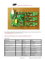
Transmitter:
The SA602 requires very little input signal to saturate. Therefore a resistor divider is placed between the audio
input from the sound card to the mixer input. This allows you to set the audio output from the sound card to a
reasonable level and not overdrive the mixer.
The other half of the LM358 (U2a) is used as a VOX circuit. The peak detector circuit of D4 and C11 isn't
required for FT8 operation, but is include if one wishes to add a VFO and microphone to use the rig as a DSB
voice transceiver or possibly try PSK31. This prevents the relay from chattering.
The output of the peak detector drives three BS170 MOSFETs. Q1 activates the T/R relay. Q2 shorts out the
antenna input to the mixer, along with connecting C9 to ground to by pass the antenna input side of the mixer
input to ground. Q5 shorts the C15/C13 junction to ground for audio muting as described earlier.
One section of the DPDT T/R relay is also used to short the receiver input to ground. Keeping as much of the
transmit signal out of the mixer input as possible is important to prevent unwanted spurious outputs. The other
half of the relay routes power to the transmitter amplifiers and lights the transmit LED.
Q7 amplifies the RF output from the mixer to a level sufficient to drive the PA. The PA is comprised of three
BS170 MOSFETS in parallel. Bias is applied to the gates to place the amplifier into liner mode. This also
reduces the amount of drive needed since the input signal does not have to first exceed the ~2.5V it takes to
start to turn on the MOSFETS.
Power to the circuits is supplied by a 9V, 1A regulator. This ensures the power output remains in a safe
operating area and if there is a problem, the internal over current protection will shut down the regulator. Since
the maximum operating voltage of the SA602/612 is 9V, a diode is placed in series with the 9V supply insure
the voltage to the chip does not exceed the maximum recommended supply voltage.
Notes:
______________________________________________________
______________________________________________________
______________________________________________________
______________________________________________________
______________________________________________________
______________________________________________________
______________________________________________________
______________________________________________________
______________________________________________________
______________________________________________________
______________________________________________________
______________________________________________________
Page 10 of 13
digital_txcvr_assembly_030720.pdf


