QRPGuys DSB Digital Transceiver Kit Manual Download Page 1


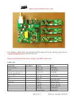
QRPGuys Digital DSB Transceiver Kit


First, familiarize yourself with the parts and check for all the components. If a part is missing, please contact us
at 

[email protected]

 and we will send you one.

Please read all the instructions before starting to assemble the transceiver.


PARTS LIST

LOCATION

QUANTITY

VALUE

TYPE

C1, C2, C10, C16 

4

10 nF -  103

X7R MMLC

C3, C6

2

100 uF /16V

Long lead plus

C4, C5, C7, C8, C9, C11, C13, 
C14, C15, C18, C21, C22

12

100 nF - 104

X7R MMLC

C12, C17, C20

3

1 uF / 25V

Long lead plus

C19

1

1 nF - 102

D1

1

1N5817

BLACK PLASTIC

D2, D3, D4

3

1N4148

SMALL GLASS

D5

1

LED Green

May have clear lens

D6

1

LED Red

May have clear lens

J1

1

BNC Jack

PCB MOUNT

J2

1

2.1mm DC Jack

PCB MOUNT

Page 1 of 13                     

digital_txcvr_assembly_030720.pdf

Summary of Contents for DSB Digital Transceiver Kit

Page 1: ...he transceiver PARTS LIST LOCATION QUANTITY VALUE TYPE C1 C2 C10 C16 4 10 nF 103 X7R MMLC C3 C6 2 100 uF 16V Long lead plus C4 C5 C7 C8 C9 C11 C13 C14 C15 C18 C21 C22 12 100 nF 104 X7R MMLC C12 C17 C20 3 1 uF 25V Long lead plus C19 1 1 nF 102 D1 1 1N5817 BLACK PLASTIC D2 D3 D4 3 1N4148 SMALL GLASS D5 1 LED Green May have clear lens D6 1 LED Red May have clear lens J1 1 BNC Jack PCB MOUNT J2 1 2 1m...

Page 2: ...12 1 47K YEL VIO ORG GLD R15 1 470 ohms YEL VIO BRN GLD U1 1 SA602 SA612A DIP 8 MIXER OSC U2 1 LM358 DIP 8 DUAL OPAMP U3 1 LM7809 TO 220 9V 1A REG V1 V2 2 6mm sq 2K TRIMMER RESISTOR T1 T2 2 FT37 43 FERITE CORE BLACK 8 PIN DIP SOCKET 2 8 Pin DIP Socket PCB 1 Main Circuit Board SCREW 1 4 40 1 4 NUT 1 4 40 nut FEET 4 Rubber Feet BAL HEADER 1 2 position SIP pin strip SHORTING JUMPER 1 Shorting jumper ...

Page 3: ...ore 2 T37 6 Yellow Core CRYSTALS 1 7 074 MHz HC 49 US 1 10 136 MHz HC 49 US 1 14 074 MHz HC 49 US MISCELLANEOUS 3 Band module boards 12 26 magnet wire 1 26 magnet wire different color 12 3 32 tie wrap J5 6 6 5 position 90 SIP pin strip Parts placement diagram Print this page for quick reference Page 3 of 13 digital_txcvr_assembly_030720 pdf ...

Page 4: ...n Blue Gold Gold R8 R10 R13 10K Brown Black Orange Gold R9 470K Yellow Violet Yellow Gold R11 680K Blue Gray Yellow Gold R12 47K Yellow Violet Orange Gold R15 470 Yellow Violet Brown Gold L4 10 uH inductor Brown Black Black Gold last band can be silver D1 1N5817 Diode black plastic body match band with outline D2 D3 D4 1N4148 Diode glass body match band with outline Capacitors C1 C2 C10 C16 10 nF ...

Page 5: ...at change R16 to 10K or 22K D5 Green LED short lead goes into hole on flat side of part outline D6 Red LED short lead goes into hole on flat side of part outline V1 V2 2K trimmer pots Relay not specifically labeled but should be obvious where it goes J2 DC power Jack J1 BNC antenna jack BAL 2 pin SIP header BALANCE not used It was found this part is not necessary Q3 Q4 Q6 These parts require some ...

Page 6: ...tin the magnet wire This is the leading cause of failure Stick the rubber bumper feet on the corners of the board Assembling the band modules Before populating with components mark each module with the band and mode in the space provided with a permanent marker J5 J6 5 pin right angle SIP header strip Short 90 pins go into board Mount on the top of the board as shown Trim the pins flush on the bac...

Page 7: ...ed by a letter C28 22 pfd marked 22 it may be followed by a letter C29 220 pfd marked 221 C30 560 pfd marked 561 C31 47 pfd marked 47 it may be followed by a letter C32 220 pfd marked 221 don t mix up the 221 and 22 values L2 18 turns on T37 2 RED core make sure turns are snug to the core and more or less evenly spaced around the core Loose winding does not work well L3 13 turns on T37 2 RED core ...

Page 8: ... use the 10A scale Set the V1 BIAS trimmer to fully CLOCKWISE Apply power to the board again Insert the shorting plug into the BAL SIP pins This will force the board into transmit mode The RED LED should now be on and the GREEN LED off Note the amount of current the board is drawing Slowly adjust the V1 trimmer COUNTERCLOCKWISE while watching the current meter Adjust until the current goes up by a...

Page 9: ... resulting in the signal flat topping At this point your creating spurious outputs to the annoyance of others in the band Keep it clean It s bad enough we re transmitting two side bands Reconnect your antenna and you are good to go Refer to the WSJT X documentation and our website links for the details on operation Theory of operation The F8 DSB transceiver is built around the ubiquitous SA602 612...

Page 10: ...er to a level sufficient to drive the PA The PA is comprised of three BS170 MOSFETS in parallel Bias is applied to the gates to place the amplifier into liner mode This also reduces the amount of drive needed since the input signal does not have to first exceed the 2 5V it takes to start to turn on the MOSFETS Power to the circuits is supplied by a 9V 1A regulator This ensures the power output rem...

Page 11: ...Page 11 of 13 digital_txcvr_assembly_030720 pdf ...

Page 12: ...Reference The following are the results for the harmonics measured on a Siglent SVA1015X 40m 30m Page 12 of 13 digital_txcvr_assembly_030720 pdf ...

Page 13: ...C s Pin 1 2 3 4 5 6 7 8 U1 1 3 1 3 0 6 8 6 8 8 2 7 9 8 33 U2 Rx 0 0 0 0 4 5 4 5 4 5 9 Mosfets and transistors Drain Gate Source Collector Base Emitter Q1 Rx 13 0 0 Q7 Rx 0 0 0 Q1 Tx 0 3 to 8 0 Q7 Tx 8 9 0 8 0 1 Q2 Rx 0 0 0 Q2 Tx 0 3 to 8 0 Q3 4 6 0 0 0 Tx 9 2 3 0 Q5 Rx 0 0 0 Q5 Tx 0 3 to 8 0 ...

Reviews: