background image

PNA-3303 User’s Manual


13

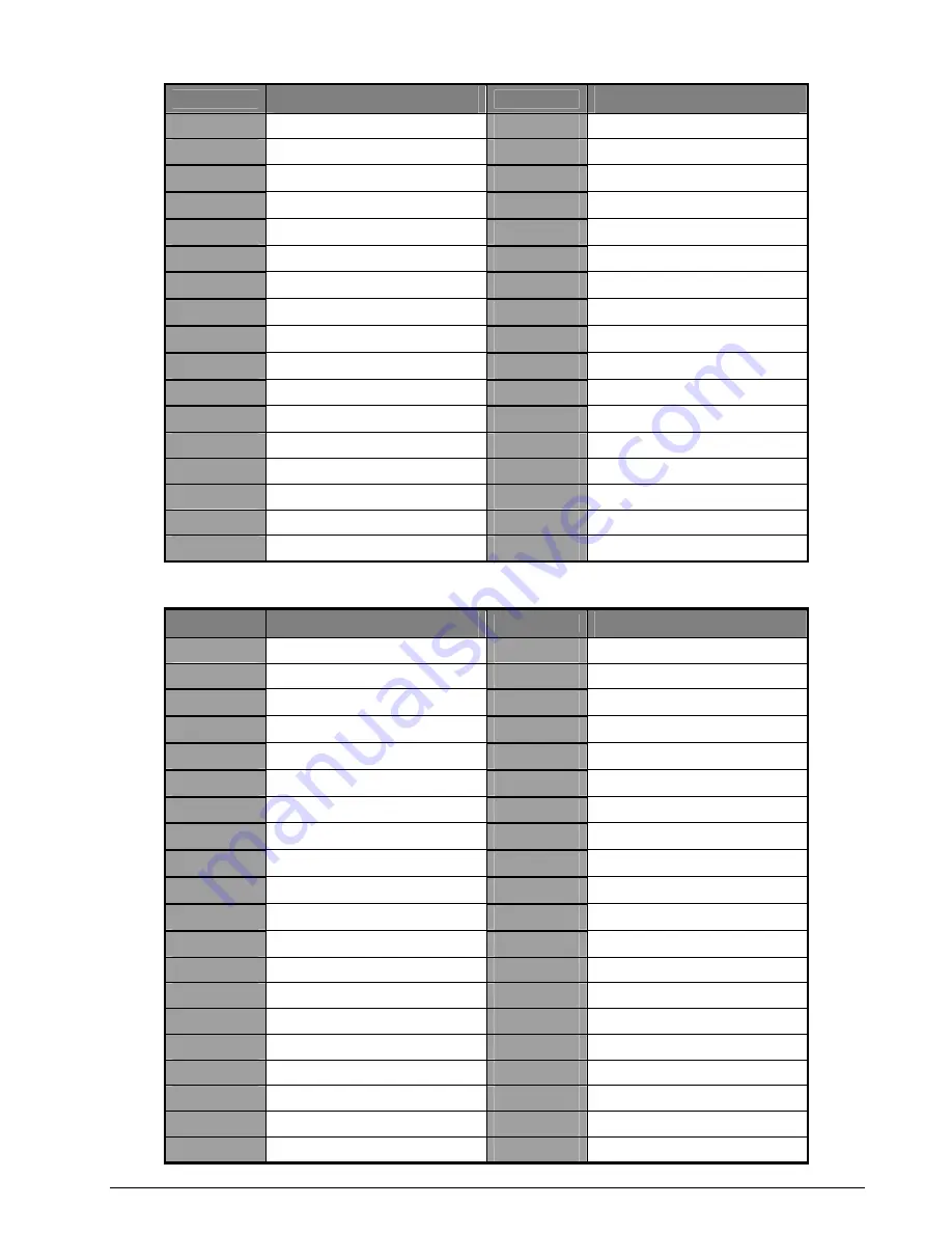
J3: FDC Connector 

PIN No. 

Signal Description 

PIN No. 

Signal Description 

Ground 

Density0# 

Ground 

N/C 

Ground 

Density1# 

Ground 

INDEX# 

Ground 

10 

MOA# 

11 

Ground 

12 

DSB# 

13 

Ground 

14 

DSA# 

15 

Ground 

16 

MOB# 

17 

Ground 

18 

DIR# 

19 

Ground 

20 

STEP# 

21 

Ground 

22 

WD# 

23 

Ground 

24 

WE# 

25 

Ground 

26 

TRACK0# 

27 

Ground 

28 

WP# 

29 

N/C 

30 

RDATA# 

31 

Ground 

32 

HEAD# 

33 

N/C 

34 

DSKCHG# 


J4/J5: IDE Connector 

PIN No. 

Signal Description 

PIN No. 

Signal Description 

RESET# 

Ground 

Data 7 

Data 8 

Data 6 

Data 9 

Data 5 

Data 10 

Data 4 

10 

Data 11 

11 

Data 3 

12 

Data 12 

13 

Data 2 

14 

Data 13 

15 

Data 1 

16 

Data 14 

17 

Data 0 

18 

Data 15 

19 

Ground 

20 

+5V 

21 

DMAREQ 

22 

Ground 

23 

IOW# 

24 

Ground 

25 

IOR# 

26 

Ground 

27 

IOCHRDY 

28 

Ground 

29 

DMAACK# 

30 

Ground 

31 

IRQ15/14 

32 

N/C 

33 

SA1 

34 

PDIAG#1CSEL 

35 

SA0 

36 

SA2 

37 

HDCCSO# 

38 

HDCCS1# 

39 

HDDACTIVE# 

40 

Ground 


Summary of Contents for PNA-3303

Page 1: ...nications Appliance Communications Appliance Communications Appliance User s Manual B8980580 Rev 001 Portwell Inc 3F No 92 Sec 1 Nei Hu Rd Taipei 114 Taiwan R O C Headquarter 886 2 2799 2020 FAX 886 2 2799 1010 http www portwell com tw Email info mail portwell com tw ...

Page 2: ...emove and Install DOM 5 2 7 Remove and Install Battery 6 2 8 Remove and Install HDD 6 2 9 Remove and Install PCI card 7 2 10 Install VGA module V 100 8 2 11 Complete the Installation 9 2 12 Product Specifications 10 2 13 Hardware Configuration Setting 11 Jumpers 11 Connectors 12 Pin Assignments of Connectors 12 2 14 Install a Different Processor 16 Install CPU 16 Remove CPU 17 Configure Processor ...

Page 3: ...le system Chapter 1 Introduction This section briefly talks about how this document is organized It includes some guidelines for users who do not want to read through everything but still helps you find what you need Chapter 2 Hardware Configuration Setting and Installation This chapter shows how the hardware is put together including detailed information It shows the definitions and locations of ...

Page 4: ...dules avoid touching their pins or gold edge fingers Put the value communications appliance system board and peripherals back into the antistatic bag when they are not in use or not installed in the chassis Some circuitry on the system board can continue operating even though the power is switched off Under no circumstances should the Lithium coin cell used to power the real time clock be allowed ...

Page 5: ...100 VGA module Fig 2 1 Front View of the Chassis Fig 2 2 Rear View of the Chassis 2 4 Open the Chassis 1 Unscrew the two screws on the bottom Fig 2 3 2 Pull out the inner steel case harder It is normal if you find it a little tight Fig 2 4 2 5 Fig 2 3 Unscrew the screws on the bottom Fig 2 4 Pull out the inner steel case step 1 3 The inner case then can be removed from the outer one Fig 2 6 Fig 2 ...

Page 6: ...socket s arm and pressing it into the slot gently Fig 2 7 2 8 Fig 2 7 The memory slot Fig 2 8 Install SODIMM 2 By pulling the arms the SODIMM can eject itself Fig 2 9 Fig 2 9 Eject a SODIMM module 2 6 Remove and Install DOM 1 Insert the DOM Fig 2 10 into the IDE interface Fig 2 11 Fig 2 10 DiskOnModule Fig 2 11 Insert DOM into IDE interface ...

Page 7: ...gertip to restore the battery Fig 2 15 Fig 2 14 Eject the battery Fig 2 15 Restore the battery 2 8 Remove and Install HDD The system has an internal drive bay for two 3 5 hard disk drives If the HDD is not pre installed you can install it by yourself Follow the steps below to install the HDD Before a HDD can be installed onto PNA 3303 PPAP 200 must be taken off from the chassis 1 Connect power cab...

Page 8: ...rd One PCI slot is available to PNA 3303 Follow the steps below for installation 1 Remove the PCI slot bracket Fig 2 20 and plug the PCI card into the PCI slot Fig 2 21 Fig 2 20 Remove the PCI slot bracket Fig 2 21 Plug in the PCI board 2 The PCI card s bracket tip is placed in the chassis corner Fig 2 22 Fix the screws back to the PCI card Fig 2 23 Fig 2 22 The PCI card s bracket tip is placed ou...

Page 9: ...V 100 module kit Fig 2 25 Fix the V 100 module onto the specific device with screws 5 The completion of V 100 kit combination Fig 2 26 6 Unscrew the screws on the back panel of PNA 3303 Fig 2 27 Fig 2 26 The completion of V 100 module kit combination Fig 2 27 Fix the V 100 module onto the specific socket with screws 7 Take off the cover on the reserved outlet for VGA connector on the back panel of...

Page 10: ... PPAP 200 The triangle sign Fig 2 30 on the connector indicates the position where pin 2 should be connected o Fig 2 31 Fig 2 32 Plug the V 100 kit to the PPAP 200 2 11 Complete the Installation 1 Pull in the inner steel case along the sliding rail Fig 2 33 If not correctly allocated it would be difficult to install Fig 2 33 Pull in the inner steel case along the sliding rail ...

Page 11: ...k Serial Ports Support two high speed 16C550 compatible UARTs with 16 byte T R FIFOs Optional Support LCD Key pad module Portwell proprietary USB Interface Support two USB ports for high speed I O peripheral devices Auxiliary I O Interfaces System reset switch power OK LED Ethernet activity LED Ethernet speed LED general purpose LED alert LED and HDD LED interface Power Input Support one DC input ...

Page 12: ...ystem board are used to select options for certain features Some of the jumpers are configurable for system enhancement The others are for testing purpose only and should not be altered To select any option cover the jumper cap over Short or remove NC it from the jumper pins according to the following instructions Here NC stands for Not Connected Please refer to Fig 2 36 for detailed jumper positi...

Page 13: ...ector J9 Serial ports connector D SUB 9 J10 Power output connector Supply power to IDE FDC Interface J11 Dual USB port connector J12 VGA board connector Need a CRT module for VGA display J13 Ethernet connector J14 Ethernet connector J15 Ethernet connector J16 CPU fan J17 Power jack J18 Right angle PCI bus connector Pin Assignments of Connectors J1 J9 Serial Port Connector PIN No Signal Description...

Page 14: ...27 Ground 28 WP 29 N C 30 RDATA 31 Ground 32 HEAD 33 N C 34 DSKCHG J4 J5 IDE Connector PIN No Signal Description PIN No Signal Description 1 RESET 2 Ground 3 Data 7 4 Data 8 5 Data 6 6 Data 9 7 Data 5 8 Data 10 9 Data 4 10 Data 11 11 Data 3 12 Data 12 13 Data 2 14 Data 13 15 Data 1 16 Data 14 17 Data 0 18 Data 15 19 Ground 20 5V 21 DMAREQ 22 Ground 23 IOW 24 Ground 25 IOR 26 Ground 27 IOCHRDY 28 G...

Page 15: ...7 J8 J16 Fan Connector PIN No Signal Description 1 Ground 2 12V 3 TachoMeter Signal J10 Power Output Connector To provide IDE FDC Interface power PIN No Signal Description 1 12V 2 Ground 3 Ground 4 5V J11 Dual USB Port Connector PIN No Signal Description PIN No Signal Description 1 5V 5 5V 2 USBD0 6 USBD0 3 USBD0 7 USBD0 4 Ground 8 Ground J12 VGA Connector PIN No Signal Description PIN No Signal D...

Page 16: ...K A2 12V B3 Ground A3 PTMS B4 N C A4 PTDI B5 5V A5 5V B6 5V A6 PIRQ B B7 PIRQ C A7 PIRQ D B8 PIRQ A A8 5V B9 N C A9 N C B10 N C A10 5V B11 N C A11 N C B12 Ground A12 Ground B13 Ground A13 Ground B14 N C A14 N C B15 Ground A15 PCIRST B16 PCICLK A16 5V B17 Ground A17 PGNT 0 B18 PREQ 0 A18 Ground B19 5V A19 N C B20 AD31 A20 AD30 B21 AD29 A21 N C B22 Ground A22 AD28 B23 AD27 A23 AD26 B24 AD25 A24 Grou...

Page 17: ... 5V B62 5V A62 5V 2 14 Install a Different Processor Install CPU 1 Lift the handling lever of CPU socket outwards and upwards to the other end 2 Align the processor pins with holes on the socket Make sure that the notched corner or dot mark pin 1 of the CPU corresponds to the socket s bevel end Then press the CPU gently until it fits into place If this operation is not easy or smooth don t do it f...

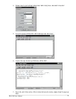
Page 18: ...s designed to self detect its CPU speed So it does not require any system adjustment 2 15 Use a Client Computer Connection Using Hyper Terminal If users use a headless PNA 3303 which has no mouse keyboard and VGA output connected to it the console may be used to communicate with PNA 3303 To access PNA 3303 via the console Hyper Terminal is one of the choices Follow the steps below for the setup 1 ...

Page 19: ...te 19200 Parity None Data bits 8 Stop bits 1 5 Turn on the power of PNA 3303 after following screen was shown 6 You can then see the boot up information of PNA 3303 7 This is the end of this section If the terminal did not port correctly please check the previous steps ...

Page 20: ...system board is eligible with Intel FC PGA Celeron and Intel FC PGA Pentium III processors and 144 pin SODIMM up to 256MB DRAM The enhanced on board PCI IDE interface supports 2 drives up to PIO mode 4 timing and Ultra DMA 100 synchronous mode feature The on board super I O chipset integrates two serial ports driven by two high performance 16C550 compatible UARTs to provide 16 byte send receive FI...

Page 21: ...nce application However the FC PGA Coppermine 256 Pentium III processor provides twice the Celeron L2 Cache The 82815 GMCH provides a completely integrated solution for the system controller and data path components in a Celeron Pentium III processor system It provides optimized 64 bit DRAM interface with one 144 pin 3 3V DIMM The 82801BA ICH2 provides a highly integrated multifunction for the bes...

Reviews: