background image

System Installation 

PEB-2131VG2A User’s Manual 


3-1 


Chapter 3  
System Installation 


This chapter provides you with instructions to set up your system. The additional 
information is enclosed to help you set up onboard PCI device and handle Watch 
Dog Timer (WDT) and operation of GPIO in software programming. 


3.1


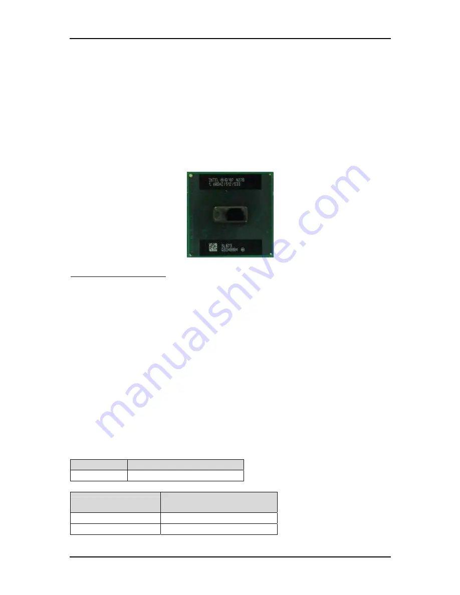
Intel ATOM


processor N270 CPU 


Configuring System Bus 

PEB-2131VG2A will automatically detect the CPU FSB 533MHz CMOS used. CPU 
speed of Intel ATOM


Processor for Mobile can be detected automatically.


3.2 Main 

Memory 

 
PEB-2131VG2A provides 1 x 200-pin SO-DIMM sockets which supports 533/400 
DDR2-SDRAM as main memory, Non-ECC (Error Checking and Correcting), non-
register functions. The maximum memory size can be up to 2GB capacity. Memory 
clock and related settings can be detected by BIOS via SPD interface. 
 
For system compatibility and stability, do not use memory module without brand. 
Watch out the contact and lock integrity of memory module with socket, it will 
impact on the system reliability. Follow normal procedures to install memory 
module into memory socket. Before locking, make sure that all modules have been 
fully inserted into the card slots. 
 

CPU FSB 

Bandwidth 

533MHz 4.2GB/s 


Memory Frequency 

Single Channel DDR 

Bandwidth 

533MHz 4.2GB/s 

400 MHz 

3.2GB/s 

Summary of Contents for PEB-2131VG2A

Page 1: ...PEB 2131VG2A Mini ITX Board User s Manual Version 1 0 Copyright Portwell Inc 2010 All rights reserved All other brand names are registered trademarks of their respective owners ...

Page 2: ...ek Gigabit Ethernet Controller 3 3 3 3 4 Audio Controller 3 3 3 4 Clear CMOS Operation 3 4 3 5 WDT Function 3 4 3 6 GPIO 3 5 Chapter 4 BIOS Setup Information 4 1 4 1 Entering Setup 4 1 4 2 Main Menu 4 2 4 3 Standard CMOS Setup Menu 4 3 4 4 IDE Adaptors Setup Menu 4 4 4 5 Advanced BIOS Features 4 6 4 6 Advanced Chipset Features 4 11 4 7 Integrated Peripherals 4 13 4 8 Power Management Setup 4 17 4 ...

Page 3: ...guide of Watch Dog Timer function Chapter 4 BIOS Setup Information Specifies the meaning of each setup parameters how to get advanced BIOS performance and update new BIOS In addition POST checkpoint list will give users some guidelines of trouble shooting Chapter 5 Troubleshooting Provides various useful tips to quickly get its running with success As basic hardware installation has been addressed...

Page 4: ...24 bit LVDS With its display enriched interface PEB 2131VG2A can support various multimedia devices and enriched IO interfaces that can supply various USB and COM devices PEB 2131VG2A supports SO DIMM memory slot for DDR2 SDRAM up to 2GB and comes with PS 2 Keyboard and Mouse header 4 x RS232 with power 2 x SATA 2 x Gigabit Ethernet 7 x USB2 0 ports It also support CompactFlash Socket and one Mini...

Page 5: ...us ports two at rear five on board for internal devices PS 2 Mouse and Keyboard Interface Support on board pin header for PS 2 keyboard mouse Audio Interface Connector of Mic in Line out Real Time Clock Calendar RTC Support Y2K Real Time Clock Calendar Watchdog Timer Support WDT function through software programming for enable disable and interval setting Generate system reset On board VGA Intel 9...

Page 6: ...ernet Chipset LAN Driver 1 Realtek RTL8168C P 8111C P PCI E Gigabit Ethernet NIC LAN Driver 2 Realtek RTL8168C P 8111C P PCI E Gigabit Ethernet NIC Audio Card Onboard Realtek ALC662 Audio Chipset Audio Driver Realtek High Definition Audio Ver 5 10 0 5735 Chip Driver Intel Chipset Device Software Ver 8 3 0 1013 USB 2 0 Driver Intel 82801G ICH7 Family USB2 Enhanced Host Controller SATA HDD WD WD2502...

Page 7: ...System Overview PEB 2131VG2A User s Manual 1 4 1 3 1 Mechanical Drawing TOP side ...

Page 8: ...System Overview PEB 2131VG2A User s Manual 1 5 Bottom side Rear IO ...

Page 9: ...System Overview PEB 2131VG2A User s Manual 1 6 1 4 System Architecture All of details operating relations are shown in PEB 2131VG2A series System Block Diagram PEB 2131VG2A System Block Diagram ...

Page 10: ...onfiguration jumpers on PEB 2131 are in the proper position The default settings are indicated with a star sign Ì 2 1 Jumper Setting For users to customize PEB 2131 s features In the following sections Short means covering a jumper cap over jumper pins Open or N C Not Connected means removing a jumper cap from jumper pins Users can refer to Figure 2 1 for the Jumper and Connector locations ...

Page 11: ...Hardware Configuration PEB 2131VG2A User s Manual 2 2 Figure 2 1 PEB 2131VG2A Jumper and Connector Locations ...

Page 12: ...TA B 5 USB DATA A 6 USB DATA B 7 Ground 8 Ground Key no pin 10 N C JP3 External PS 2 Keyboard Mouse Pin Header PIN No Signal Description PIN No Signal Description 1 Mouse Data 2 Keyboard Data Key no pin Key no pin 5 Ground 6 Ground 7 Power 8 Power 9 Mouse CLK 10 Keyboard CLK JP5 POWER LED HDD LED Pin Header PIN No Signal Description 1 Power LED 2 Power LED 3 HDD LED 4 HDD LED JP6 System Reset Powe...

Page 13: ...WER Input 6 GPIO56 7 GPIO53 8 GPIO57 9 GND 10 5V JP11 PANEL BACKLIGHT Selection Pin No Signal Description 1 3 2 4 5V Active High Ì 1 3 4 6 12V Active High 3 5 2 4 5V Active Low 3 5 4 6 12V Active Low JP12 LVDS Panel VDD input voltage selection JP12 Function 2 4 short VDD 3 3V Ì 3 4 short VDD 12V 4 6 short VDD 5V Note Wrong voltage selection may damage the LVDS panel Please survey LVDS panel s VDD ...

Page 14: ...port device s RI before setup this jumper setting JP15 COM3 COM4 Port RI Voltage selection JP15 Function 1 3 short VDD 5V For COM 3 port RI Voltage Ì 3 5 short VDD 12V For COM3 port RI Voltage 2 4 short VDD 5V For COM4 port RI Voltage Ì 4 6 short VDD 12V For COM4 port RI Voltage Note Wrong voltage selection may damage the COM Port device Please survey COM port device s RI before setup this jumper ...

Page 15: ...List Connector Function Remark J1 DDR2 DIMM J2 Battery connector J3 USB Dual Connector J4 J5 SATA Connector J6 RJ45 LAN2 Connector J7 CRT Connector J8 CF Connector J9 Mini PCI E Socket J10 COM2 Pin Header 2x5P _2 0mm J11 System FAN J12 LVDS Connector DF13 30DP J13 J14 J15 COM1 COM3 COM4 Pin Header 2x5P _2 0mm J16 Audio JACK LINE_OUT J17 Audio LINE_OUT LINE_IN MIC Pin HDR Wafer 2mm J18 RJ45 LAN1 Co...

Page 16: ...ignal Description PIN No Signal Description 1 WAKE 2 3 3V 3 N C 4 GND 5 N C 6 1 5V 7 CLKREQ 8 N C 9 GND 10 N C 11 PCI E _CLK 12 N C 13 PCI E_CLK 14 N C 15 GND 16 N C KEY NO Pin KEY NO Pin 17 N C 18 GND 19 N C 20 N C 21 GND 22 RESET 23 PCI E_RX 24 3V_UDAL 25 PCI E_RX 26 GND 27 GND 28 1 5V 29 GND 30 SMB_CLK 31 PCI E_TX 32 SMB_DATA 33 PCI E _TX 34 GND 35 GND 36 USB_DATA 37 N C 38 USB_DATA 39 N C 40 G...

Page 17: ...1 LCD1DO0 2 LCD1DO0 3 LCD1DO1 4 LCD1DO1 5 LCD1DO2 6 LCD1DO2 7 LCD1DO3 8 LCD1DO3 9 LCD1CLK 10 LCD1CLK 11 LCD2DO0 12 LCD2DO0 13 LCD2DO1 14 LCD2DO1 15 LCD2DO2 16 LCD2DO2 17 LCD2DO3 18 LCD2DO3 19 LCD2CLK 20 LCD2CLK 21 LCLK1 22 LDATA1 23 GND 24 N C 25 GND 26 GND 27 LVDS VDD 28 LVDS VDD 29 N C 30 LVDS VDD 9 GND 10 GND J17 Audio LINE_OUT LINE_IN MIC Pin HDR PIN No Signal Description PIN No Signal Descrip...

Page 18: ...Hardware Configuration PEB 2131VG2A User s Manual 2 9 J19 POWER DC 12V Connector PIN No Signal Description 1 GND 2 GND 3 12V 4 12V ...

Page 19: ...A provides 1 x 200 pin SO DIMM sockets which supports 533 400 DDR2 SDRAM as main memory Non ECC Error Checking and Correcting non register functions The maximum memory size can be up to 2GB capacity Memory clock and related settings can be detected by BIOS via SPD interface For system compatibility and stability do not use memory module without brand Watch out the contact and lock integrity of mem...

Page 20: ...ck all jumpers setting on proper position Step 2 Install and configure memory module on right position Step 3 Place PEB 2131VG2A into the dedicated position in the system Step 4 Attach cables to existing peripheral devices and secure it WARNING Please ensure that SBC is properly inserted and fixed by mechanism Note Please refer to section 3 3 1 to 3 3 4 to install INF VGA LAN Audio drivers 3 3 1 C...

Page 21: ... find Springdale GMCH driver in the PEB 2131VG2A CD title Drivers support Windows 2000 Windows XP 3 3 3 Realtek Gigabit Ethernet Controller Drivers Support Please find Realtek RTL8111C LAN driver in Ethernet directory of PEB 2131VG2A CD title The drivers support Windows 2000 XP LED Indicator for LAN status PEB 2131VG2A provides two LED indicators to report Realtek RTL8111C Gigabit Ethernet interfa...

Page 22: ...ndex Register for identifying CR index number 2 0x2F EFDR Extended Function Data Register for accessing desired CR Below are some example codes which demonstrate the use of WDT Enter Extended Function Mode outp 0x002E 0x87 outp 0x002E 0x87 Select Logic Device 8 outp 0x002E 0x07 outp 0x002F 0x08 Assign Pin 77 WDTO Enable outp 0x002E 0x30 outp 0x002F inp 0x002F 0x01 Select Count Mode outp 0x002E 0xF...

Page 23: ...6 GPIO GPIO From Super I O The PEB 2131VG2A provides 4 input output ports from SIO that can be individually configured to perform a simple basic I O function Users can configure each individual port to become an input or output port by programming register bit of I O Selection To invert port value the setting of Inversion Register has to be made Port values can be set to read or write through Data...

Page 24: ...s which demonstrate the use of GPIOs Enter Extended Function Mode outp 0x002E 0x87 outp 0x002E 0x87 Assign Pin1 4 and Pin125 128 to be GPIO port 1 outp 0x002E 0x29 outp 0x002F 0x7F Select Logic Device 8 outp 0x002E 0x07 outp 0x002F 0x08 Active GPIO 5 outp 0x002E 0x30 outp 0x002F 0x03 Select I O Mode outp 0x002E 0xE0 outp 0x002F inp 0x002F 0xF0 I O Selection Register 0x0F Select Inversion Mode outp...

Page 25: ...he same as in Data Register Value of I O Selection Register Only lower nibble is available for this function When set to a 1 respective GPIO port is programmed as an input port When set to a 0 respective GPIO port is programmed as an output port Value of Output Data Input Data Only lower nibble is available for this function If a port is assigned to be an output port then its respective bit can be...

Page 26: ...r reboot the computer When the message Hit DEL if you want to run SETUP appears press Del key immediately to enter BIOS setup program If the message disappears before you respond but you still wish to enter Setup please restart the system to try COLD START again by turning it OFF and then ON or touch the RESET button You may also restart from WARM START by pressing Ctrl Alt and Delete keys simulta...

Page 27: ...g up the sub menu Phoenix AwardBIOS CMOS Setup Utility f Standard CMOS Features f Advanced BIOS Features f Advanced Chipset Features f Integrated Peripherals f Power Management Setup f PnP PCI Configurations f PC Health Status Load Fail Safe Defaults Load Optimized Defaults Set Supervisor Password Set User Password Save Exit Setup Exit Without Saving ESC Quit Select Item F10 Save Exit Setup Time D...

Page 28: ...tection Status Phoenix AwardBIOS CMOS Setup Utility Standard CMOS Features Item Help Date mm dd yy Tue Nov 24 2009 Time hh mm ss 10 20 30 f IDE Channel 0 Master None f IDE Channel 0 Slave None f IDE Channel 1 Master None f IDE Channel 1 Slave None Video EGA VGA Halt On All But Keyboard Base Memory 639K Extended Memory 1038336K Total Memory 1039360K Menu Level f Change the day month year and centur...

Page 29: ...Memory N A Displays the amount of extended memory detected during boot up Total Memory N A Displays the total memory available in the system 4 4 IDE Adaptors Setup Menu The IDE adapters control the SATA devices such as hard disk drive or CD ROM drive It uses a separate sub menu to configure each hard disk drive Phoenix AwardBIOS CMOS Setup Utility IDE Channel 0 Master Slave Item Help IDE HDD Auto ...

Page 30: ...e PRECOMP 65535 means NONE Access Mode CHS LBA Large Auto Choose the access mode for this hard disk Capacity Auto Display your disk drive size Disk drive capacity Approximated Note that this size is usually slightly greater than the size of a formatted disk given by a disk checking program The following options are selectable only if the IDE Primary Master item is set to Manual Cylinder Min 0 Max ...

Page 31: ...oot Other Device Enabled Boot up NumLock Status On Gate A20 Option Fast Typematic Rate Setting Disabled X Typematic Rate Chars Sec 6 X Typematic Delay Msec 250 Security Option Setup X APIC Mode Enabled MPS Version Control For OS 1 4 OS Select For DRAM 64MB Non OS2 Report No FDD For WIN 95 No Full Screen LOGO Show Disabled Small Logo EPA Show Disabled Menu Level f Move Enter Select PU PD Value F10 ...

Page 32: ...ther to limit CPUID maximum value The choice Enabled Disabled C1E Function CPU C1E Function Select The choice Auto Disabled Execute Disabled Bit When disabled forces the XD feature flag to always return 0 The choice Enabled Disabled Phoenix AwardBIOS CMOS Setup Utility Hard Disk Boot Priority Item Help 1 Bootable ADD in Cards Menu Level f Use or to select a device then press to move it up or to mo...

Page 33: ...d disk partition table CPU L1 L2 Cache This setting enables the CPU internal cache L1 L2 cache The choice Enabled Disabled Hyper Threading Technology Please note that this feature is only working for operating system with multi processors mode supported The choice Enabled Disabled Quick Power On Self Test Allows the system skip certain tests while booting This will decrease the time needed to boot...

Page 34: ...tic delay Msec The delay before keystrokes begin to repeat The choice 250 500 750 and 1000 Default 250 Security Option Select whether the password is required every time the system boots or only when you enter setup System The system will not boot and access to Setup will be denied if the correct password is not entered at the prompt Setup The system will boot but access to Setup will be denied if...

Page 35: ...m with greater than 64MB of RAM on the system The choice Non OS2 OS2 Report No FDD for WIN 95 Select Yes to release IRQ6 when the system contains no floppy drive for compatibility with Windows 95 logo certification In the Integrated Peripherals screen select Disabled for the Onboard FDD Controller field The choice No Yes Full Screen LOGO Show The choice Enabled Disabled Small Logo EPA Show The cho...

Page 36: ... DRAM Timing Selectable By SPD X CAS Latency Time Auto X DRAM RAS to CAS Delay Auto X DRAM RAS Precharge Auto X Precharge dealy tRAS Auto X System memory Frequency Auto SLP_S4 Assertion Width 4 to 5 Sec System BIOS Cacheable Enabled Video BIOS Cacheable Disabled Memory Hole At 15M 16M Disable f PCI Express Root port Func press Enter VGA Setting On Chip Frame Buffer Size 8MB DVMT Mode DVMT DVMT FIX...

Page 37: ...ot port Func The choice Auto Enabled Disabled On Chip Frame Buffer Size Users can set the display memory size that shared from main memory The choice 1MB 8MB DVMT Mode The choice FIXED DVMT BOTH DVMT FIXED Memory The choice 64MB 128MB 224MB Boot Display The choice CRT LVDS CRT LVDS Panel Scaling The choice Auto On Off Panel Number The choice 800X600 18bit 1ch 1024X768 18bit 1ch 1024X768 24bit 2ch ...

Page 38: ...ode Enabled IDE DMA transfer access Enabled On Chip Primary PCI IDE Enabled IDE Primary Master PIO Auto IDE Primary Slave PIO Auto IDE Primary Master UDMA Auto IDE Primary Slave UDMA Auto On Chip Secondary PCI IDE Enabled IDE Secondary Master PIO Auto IDE Secondary Slave PIO Auto IDE Secondary Master UDMA Auto IDE Secondary Slave UDMA Auto On Chip Serial ATA Setting On Chip Serial ATA Combined Mod...

Page 39: ...orts Modes 0 through 4 provide successively increased performance In Auto mode the system automatically determines the best mode for each device The choice Auto Mode 0 Mode 1 Mode 2 Mode 3 Mode 4 IDE Primary Secondary Master Slave UDMA Ultra DMA 33 66 100 implementation is possible only if IDE hard drive supports and the operating environment includes a DMA driver Windows 95 OSR2 or a third party ...

Page 40: ...erial bus Move Enter Select PU PD Value F10 Save ESC Exit F1 General Help F5 Previous Values F6 Fail Safe Defaults F7 Optimized Defaults USB Controller Enabled or Disabled Universal host controller interface for universal serial bus The choice Enabled Disabled USB 2 0 Controller Enabled or Disabled Enhanced host controller interface for universal serial bus The choice Enabled Disabled USB Keyboard...

Page 41: ...e ESC Exit F1 General Help F5 Previous Values F6 Fail Safe Defaults F7 Optimized Defaults Onboard Serial Port 1 Port 2 Port 3 Port 4 The choice Disabled 3F8 2F8 3E8 2E8 Onboard UART Port 1 Port 2 Port 3 Port 4 The choice IRQ4 IRQ3 IRQ5 IRQ10 IRQ9 IRQ7 IRQ11 PWRON After PWR Fail This item allows user to configure the power status of using ATX power supply after a serious power loss occurs The choic...

Page 42: ...uspend Yes Suspend Type Stop Grant Suspend Mode Disabled HDD Power Down Disabled Soft Off by PWR BTTN Instant Off Wake Up by Onboard LAN Enabled Resume by Alarm Disabled X Date of Month Alarm 0 X Time hh mm ss Alarm 0 0 0 Reaload Global Tumer Events Primary IDE 0 Disabled Primary IDE 1 Disabled Secondary IDE 0 Disabled Secondary IDE 1 Disabled FDD COM LPT Port Disabled PCI PIRQ A D Disabled Menu L...

Page 43: ...ed Allows you to set each mode individually When not disabled Suspend Mode ranges from 1 min to 1 Hour and HDD Power Down ranges from 1 Min to 15 Min Video off Method This determines the manner in which the monitor is blanked V H SYNC Blank This selection will cause the system to turn off the vertical and horizontal synchronization ports and write blanks to the video buffer Blank Screen This optio...

Page 44: ...ed Resume by Alarm This item allows users to enable disable the resume by alarm function When Enabled is selected system using ATX power supply could be powered on if a customized time and day is approached The choice Enabled Disabled Date of Month Alarm When Resume by Alarm is enabled this item could allow users to configure the date parameter of the timing dateline on which to power on the syste...

Page 45: ...which allows I O devices to operate at speeds nearing the speed the CPU itself uses when communicating with its own special components This section covers some very technical items and it is strongly recommended that only experienced users should make any changes to the default settings Phoenix AwardBIOS CMOS Setup Utility PnP PCI Configurations Item Help Init Display First Onboard Reset Configura...

Page 46: ...ected since BIOS automatically assigns them The choice Auto ESCD Manual IRQ Resources When resources are controlled manually assign each system interrupt a type depending on the type of device using the interrupt The choice Press Enter IRQ 3 IRQ 4 IRQ 5 IRQ 7 IRQ 9 IRQ 10 IRQ 11 IRQ 12 IRQ 14 IRQ 15 assigned to The choice PCI Device Reserved PCI VGA Palette Snoop Legacy ISA for devices compliant w...

Page 47: ...mart Fan Temp Disabled X Fan Tolerance Value 5 Menu Level f Move Enter Select PU PD Value F10 Save ESC Exit F1 General Help F5 Previous Values F6 Fail Safe Defaults F7 Optimized Defaults CPU Warning Temperature This item allows you to set a temperature above which the system will start the beeping warning Default setting is disabled This function will only with ACPI power management and S3 STR sus...

Page 48: ...be setup or both of then The differences between are Set Supervisor Password can enter and change the options of the setup menus Set User Password just can only enter but do not have the right to change the options of the setup menus When selecting this function the following message will appear at the center of the screen to assist you in creating a password ENTER PASSWORD Type the password up to...

Page 49: ...System the password will be required both at boot and at entry to Setup If set to Setup prompting only occurs when trying to enter Setup 4 13 Exiting Selection Save Exit Setup Pressing Enter on this item asks for confirmation Save to CMOS and EXIT Y N Y Pressing Y stores the selections made in the menus in CMOS a special section of memory that stays on after system off During subsequnet booting of...

Page 50: ...ng with success As basic hardware installation has been addressed in Chapter 2 this chapter will primarily focus on system integration issues in terms of BIOS setting and OS diagnostics 5 1 Hardware Quick Installation DC 12V Power Input Unlike other Single board computer PEB 2131VG2A supports DC 12V Power J20 or 4 Pin 12V Power J19 Figure J20 J19 ...

Page 51: ... malfunction of any device To make sure that you have a successful start with PEB 2131VG2A it is recommended when going with the boot up sequence to hit DEL key and enter the BIOS setup menu to tune up a stable BIOS configuration so that you can wake up your system far well Loading the default optimal setting When prompted with the main setup menu please scroll down to Load Optimal Defaults press ...

Page 52: ...ource A few good examples are Disable COM1 serial port to release IRQ 4 Disable COM2 serial port to release IRQ 3 Etc A quick review of the basic IRQ mapping is given below for your reference IRQ Description IRQ 0 System Counter IRQ 1 Keyboard IRQ 2 Programmed Controller IRQ 3 COM2 IRQ 4 COM1 IRQ 5 Display Network USB 1 0 1 1 UHCI Controller IRQ 6 Floppy Disk Controller IRQ 7 Printer Port Parallel...

Page 53: ... it inserts properly Beep rapidly Power error warning Please check Power mode setting Installation Problem Question How do I connect my keyboard and mouse as there is only one connector Answer Users may always adopt PS 2 keyboard and mouse over the PS 2 interface JP3 on PEB 2131VG2A Question I forget my password of system BIOS what am I supposed to do Answer You can simply short 2 3 pins on JP1 to...

Page 54: ...d Memory Area Size Device Description 0000 003F 1K Interrupt Area 0040 004F 0 3K BIOS Data Area 0050 006F 0 5K System Data 0070 0E2E 54K DOS 0E2F 0F6B 5K Program Area 0F6C 9EFF 574K Available Conventional memory ends at 640K 9F00 9FBF 3K Unused 9FC0 9FFF 1K Extended Bios Area A000 AFFF 64K VGA Graphics B000 B7FF 32K Unused B800 BFFF 32K VGA Text C000 CEBF 59K Video ROM CEC0 EFFF 133K Unused F000 F...

Page 55: ...ROM System Timer IRQ 1 System ROM Keyboard Event IRQ 2 Unassigned Usable IRQ IRQ 3 System ROM COM 2 IRQ 4 System ROM COM 1 IRQ 5 Unassigned Usable IRQ IRQ 6 System ROM Diskette Event IRQ 7 Unassigned Usable IRQ IRQ 8 System ROM Real Time Clock IRQ 9 Unassigned Usable IRQ IRQ 10 Unassigned Usable IRQ IRQ 11 Unassigned Usable IRQ IRQ 12 System ROM IBM Mouse Event IRQ 13 System ROM Coprocessor Error ...

Reviews: