132
PDP-433CMX
1
2
3
4
C
D
F
A
B
E
1
2
3
4
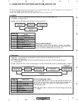
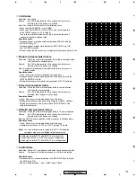
The PD history displayed in "INFORMATION" of the Factory menu.
Display of PD point
Time stamp display
[OOOOOH] : HOUR, [OOM] : MINUTE
Example:
Time stamp display is [65432H10M]
→
65432 hours 10 minutes
Time stamp data
upper 5 byte: HOUR, lower 2 byte: MINUTE
Example:
Time stamp is [6543210]
→
65432 hours 10 minutes
The data (1st/2nd/time stamp) on the past eight power-downs are stored in memory.
Diagnosis Method in Power Down
1
OSD display of the PD history
2
Retrieval of PD history by RS-232C command "GPD"
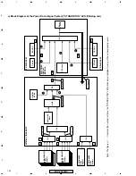
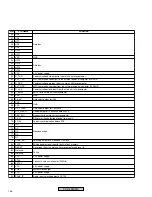
Power-Down Point
OSD Display
Y-DRIVE
Y-DRV
Y-DC/DC COVERTER
Y-DDC
X-DC/DC CONVERTER
X-DDC
X-DRIVE
X-DRV
Power supply
POWER
ADDRESS junction
ADRES
ADDRESS resonance
ADR-K
DC/DC CONVERTER (DIGITAL)
DC-DC
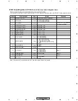
Data of PD point
Power-Down Point
"GPD" Data
Y-DRIVE
1
Y-DC/DC COVERTER
2
X-DC/DC CONVERTER
3
X-DRIVE
4
Power supply
5
ADDRESS junction
6
ADDRESS resonance
7
DC/DC CONVERTER (DIGITAL)
8
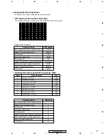
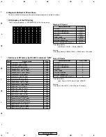
Order
Data contents
Size
1
The latest "1st PD" point
1 byte
2
The latest "2nd PD" point
1 byte
3
The latest PD time stamp
7 byte
4
Second latest "1st PD" point
1 byte
5
Second latest "2nd PD" point
1 byte
6
Second latest PD time stamp
7 byte
7
Third latest "1st PD" point
1 byte
8
Third latest "2nd PD" point
1 byte
9
Third latest PD time stamp
7 byte
10
Fourth latest "1st PD" point
1 byte
11
Fourth latest "2nd PD" point
1 byte
12
Fourth latest PD time stamp
7 byte
13
Fifth latest "1st PD" point
1 byte
14
Fifth latest "2nd PD" point
1 byte
15
Fifth latest PD time stamp
7 byte
16
Sixth latest "1st PD" point
1 byte
17
Sixth latest "2nd PD" point
1 byte
18
Sixth latest PD time stamp
7 byte
19
Seventh latest "1st PD" point
1 byte
20
Seventh latest "2nd PD" point
1 byte
21
Seventh latest PD time stamp
7 byte
22
Eighth latest "1st PD" point
1 byte
23
Eighth latest "2nd PD" point
1 byte
24
Eighth latest PD time stamp
7 byte
I N
PD
F
1
X
DDC
0 5 1 4 8 H 2 5 M
0 2 2 4 8 H 1 4 M
0 1 3 5 8 H 3 6 M
0 0 3 4 8 H 1 5
0 0 0 0 0
0 0
0 0 0 0 0
0 0
0 0 0 0 0
0 0
0 0 0 0 0
0 0
M
2
A D R – K
3
Y
DR V
4
–
X – DDC
D
– DC
C
A D R E S
–
5
– – – – –
– – – – –
– – – – –
– – – – –
6
7
8
H
H
H
H
M
M
M
M
– – – – –
– – – – –
– – – – –
– – – – –
– – – – –
– – – – –
O
I N FO
1 S T
2 ND
–
–
S 1
I N 4 – 0 2 –
∗
2
N T
# 1
1
1
5
10
15
16
5
10
15
20
25
30
32
Summary of Contents for PDP 433CMX
Page 165: ...165 PDP 433CMX Pin Assignment Top View CXA3516R RGB ASSY IC4603 AD PLL IC ...
Page 166: ...166 PDP 433CMX Block Diagram ...
Page 167: ...167 PDP 433CMX Pin Function ...
Page 168: ...168 PDP 433CMX ...
Page 169: ...169 PDP 433CMX ...

