background image

130

PDP-433CMX

1

2

3

4

C

D

F

A

B

E

1

2

3

4

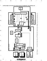
Address PD

Mute

DIGITAL

DC-DC

X Drive

X DC-DC

OR

OR

PD Circuit

Y Drive

Y DC-DC

OR

Relay

Circuit

AND

OR

OR

OR

D8

D11

8

6

7

4

5

1

2

3

ADR CONNECT

ASSY

(Upper)

DIGITAL VIDEO ASSY

SW POWER

SUPPLY

MODULE

X DRIVE ASSY

Y DRIVE ASSY

ADR CONNECT

ASSY

(Lower)

RESONANCE

ASSY

(Upper)

RESONANCE

ASSY

(Lower)

-

D12

D16

D1

X1

P4

P2

P3

Y1

D17

D15

-

IC1201-pin 8

IC1201-pin 6

D1202 Cathode

DIG_ADR.PD

PD_TRIGGER

Note: The figures 

1

 - 

8

 indicate the number of times the "STANDBY/ON" LED blinks when shutdown occurs in the corresponding route.

Block Diagram of the Power Down Signal System ("STANDBY/ON" LED: Blinking red)

Summary of Contents for PDP 433CMX

Page 1: ... MANUAL IS APPLICABLE TO THE FOLLOWING MODEL S AND TYPE S This Service Manual should be used together with the following manual s Model No Order No Remarks PDP 433CMX PDP 433MXE ARP3156 SCHEMATIC DIAGRAM and PCB DIAGRAM Model No Part numbers and serial numbers of the main parts applicable to this service manual SW POWER SUPPLY MODULE AXY1059 Rear Case ANE1608 RGB ASSY AWZ6744 DIGITAL VIDEO ASSY AW...

Page 2: ...3 When service is required observe the original lead dress Extra precaution should be taken to assure correct lead dress in the high voltage circuitry area 4 Always use the manufacture s replacement components Especially critical components as indicated on the circuit diagram should not be replaced by other manufacture s Furthermore where a short circuit has occurred replace those components that ...

Page 3: ...easured must not exceed 0 5mA ANY MEASUREMENTS NOT WITHIN THE LIMITS OUTLINED ABOVE ARE INDICATIVE OF A POTENTIAL SHOCK HAZARD AND MUST BE CORRECTED BEFORE RETURNING THE SET TO THE CUSTOMER PRODUCT SAFETY NOTICE Many electrical and mechanical parts in PIONEER set have special safety related characteristics These are often not evident from visual inspection nor the protection afforded by them neces...

Page 4: ...er In the SW POWER SUPPLY Module 6 Other primary side of the SW POWER SUPPLY Module CHARGED SECTION AND HIGH VOLTAGE GENERATING POINT 7 High Voltage Generating Point The places where voltage is 100V or more except for the charged places described above If the places are touched there is a risk of electric shock 1 SW POWER SUPPLY Module 215V 2 X DRIVE Assy 280V to 215V 3 Y DRIVE Assy 345V 4 SCAN A ...

Page 5: ...s glues and replacement parts Appropriately applying grease or glue can maintain the product performances But improper lubrication or applying glue may lead to failures or troubles in the product By following the instructions in this manual be sure to apply the prescribed grease or glue to proper portions by the appropriate amount For replacement parts or tools the prescribed ones should be used 4...

Page 6: ...Y 37 3 1 5 Y DRIVE ASSY 38 3 1 6 MX AUDIO ASSY 40 3 1 7 SUB ADDRESS A and B ASSYS 41 3 1 8 ADR RESONANCE ASSY 42 3 1 9 ADR CONNECT A B C and D ASSYS 42 3 1 10 VIDEO SIGNAL ROUTE 43 3 1 11 SYNC SIGNAL ROUTE 44 3 2 WAVEFORMS 45 4 PCB CONNECTION DIAGRAM Refer to ARP3156 5 PCB PARTS LIST 54 6 ADJUSTMENT 68 6 1 SERVICE FACTORY MODE 68 6 1 1 State Transition Diagram 6 1 2 Table of Adjustment Items in Se...

Page 7: ...eo INPUT 1 Input Mini D sub 15 pin socket connector RGB signal G ON SYNC compatible RGB 0 7 Vp p 75 Ω no sync HD CS VD TTL level positive and negative polarity 2 2 kΩ G ON SYNC 1 Vp p 75 Ω negative sync Compatible with Microsoft s Plug Play VESA DDC1 2B Output Mini D sub 15 pin socket connector 75 Ω with buffer INPUT 2 Input BNC jack x5 RGB signal G ON SYNC compatible RGB 0 7 Vp p 75 Ω no sync HD ...

Page 8: ...when replacing be sure to use parts of identical designation Screws adjacent to mark on the product are used for disassembly For the applying amount of lubricants or glue follow the instructions in this manual In the case of no amount instructions apply as you think it appropriate 10 18 3 1 27 6 5 2 7 27 20 21 22 33 11 14 12 13 34 35 32 29 25 24 31 30 26 36 28 4 2 8 23 PDP 433CMX Only PDP 433MXE O...

Page 9: ...ating Instructions See Contrast table 2 Japanese English French 34 Operating Instructions See Contrast table 2 Spanish Italian Dutch 35 Operating Instructions See Contrast table 2 English French German 36 Ferrite Core See Contrast table 2 37 Warranty Card Contens Label See Contrast table 2 2 CONTRAST TABLE PDP 433CMX LUCB and PDP 433MXE YVLDK are constructed the same except for the following Mark ...

Page 10: ...10 PDP 433CMX 2 2 UNDER LAYER SECTION 1 Upper side 9 1 11 11 11 11 11 11 11 11 10 10 11 11 10 10 5 or 6 9 7 or 8 1 2 3 4 2 3 4 12 13 13 13 13 13 ...

Page 11: ...WZ6730 NSP 8 BRIDGE D Assy AWZ6731 NSP 9 ADR RESONANCE Assy AWZ6751 10 Screw ABA1301 11 Screw VBB30P100FNI 12 Shading Sheet 43 AMR3313 13 Rear Coner Label AAX2862 Mark No Description Part No UNDER LAYER SECTION 1 PARTS LIST 2 3 UNDER LAYER SECTION 2 1 Panel Chassis 43 Assy AWU1067 Refer to 2 17 PANEL CHASSIS 43 ASSY 2 Circuit Board Spacer AEC1872 3 Circuit Board Spacer AEC1873 NSP 4 PCB Spacer AEC...

Page 12: ...12 PDP 433CMX 2 4 UNDER LAYER SECTION 3 11 Upper side 1 13 13 4 5 6 5 4 13 14 15 Upper side Upper side Upper side 11 14 X DRIVE Assy 14 12 2 3 14 14 9 8 ...

Page 13: ...UDIO Assy AWZ6644 NSP 4 Metal Fitting ANG2464 NSP 5 Heat Sink ANH1594 6 Silicone Sheet AEH1039 7 8 Audio Sheet 43 AMR3285 9 Rivet BEC1066 10 11 Coil Silicone Sheet AEH1048 12 Circuit Board Spacer AEC1872 13 Screw ABZ30P060FMC 14 Screw VBB30P100FNI 15 Screw PMB30P060FNI UNDER LAYER SECTION 3 PARTS LIST ...

Page 14: ...14 PDP 433CMX Upper side 8 9 1 Upper side Upper side 9 7 5 6 2 10 10 8 8 2 5 UNDER LAYER SECTION 4 ...

Page 15: ...oard Spacer AEC1872 3 4 5 Scan IC Spring 43L ABK1029 6 Scan IC Spring 43R ABK1030 7 Scan Insulation Sheet 43 AMR3287 8 Screw VBB30P100FNI 9 Screw PMB30P060FNI 10 Coil Silicone Sheet AEH1048 UNDER LAYER SECTION 4 PARTS LIST Mark No Description Part No ...

Page 16: ...16 PDP 433CMX 2 6 UNDER LAYER SECTION 5 Upper side Bottom View 10 5 6 2 3 6 7 5 7 10 10 7 4 1 8 9 7 18 15 11 18 10 20 Wire Saddle Wire Saddle Fan Jumper 19 10 14 13 12 14 14 14 11 10 17 10 15 ...

Page 17: ...re Saddle AEC1904 NSP 8 PCB Spacer AEC1121 9 Circuit Board Spacer AEC1873 10 Screw ABZ30P060FMC 11 Fan Motor AXM1040 NSP 12 Fan Metal L ANG2488 NSP 13 Fan Metal R ANG2489 14 Screw PPZ50P100FZK 15 Screw BMZ30P060FZK 16 17 Niplocker AEC1803 18 Fan Label AAX2785 19 J115 3P Housing Wire ADX2780 20 Binder AEC 093 UNDER LAYER SECTION 5 PARTS LIST Mark No Description Part No ...

Page 18: ...11 D15 D14 D13 D12 D17 SA1 SA2 X1 TE1 SA2 SA1 D6 D7 D2 D3 D8 D9 K3 K3 A6 A7 A5 A1 A3 Upper side 1 39 27 27 27 27 31 29 16 2 10 27 30 36 5 3 4 17 43 33 38 18 1 39 21 22 23 27 24 2 3 46 4 14 13 12 37 35 15 27 27 8 11 5 9 19 27 32 6 7 46 28 34 45 44 20 27 40 42 25 26 ...

Page 19: ...10 Flexible Flat Cable ADD1204 23 J211 Flexible Flat Cable ADD1199 24 J212 Flexible Flat Cable ADD1201 25 J201 Flexible Flat Cable ADD1183 UNDER LAYER SECTION 6 PARTS LIST Mark No Description Part No Mark No Description Part No 26 J202 Flexible Flat Cable ADD1183 27 Flat Clamp AEC1879 28 J203 Flexible Flat Cable ADD1198 29 J205 Flexible Flat Cable ADD1202 30 J206 Flexible Flat Cable ADD1200 31 J20...

Page 20: ...DLE LAYER SECTION 1 PARTS LIST Mark No Description Part No Upper side Upper side 10 10 11 11 10 6 11 11 1 7 5 3 2 11 2 Upper side Upper side 12 12 11 8 9 9 11 14 14 4 11 11 8 11 13 15 2 8 MIDDLE LAYER SECTION 1 Mark No Description Part No NSP 8 Front Chassis V 43 ANA1672 9 FPC Cushion 43 AEB1371 10 Screw ABA1283 11 Screw ABA1294 12 Screw BMZ30P060FMC 13 VR Cushion AEB1374 14 V Cushion AED1205 15 G...

Page 21: ...MX LED Assy AWZ6642 3 J113 Wire O ADX2778 4 KEY CONNECTOR Assy AWZ6695 NSP 5 IR Holder ANG2494 6 Nyron Rivet AEC1671 7 J111 Wire Y ADX2788 NSP 8 Switch Holder ANG2493 9 Screw BMZ30P040FMC 10 11 V Cushion AED1205 12 Gascket R ANK1695 MIDDLE LAYER SECTION 2 PARTS LIST Mark No Description Part No ...

Page 22: ...round Finger ANG2468 7 Card Spacer AEC1899 8 Ferrite Core L3 ATX1037 9 Ferrite Core Holder AEC1818 10 J112 13P Housing Wire ADX2784 11 Guide Rail EX AEC1900 12 Clamp AEC1884 13 J107 12P Housing Wire ADX2702 14 J109 Wire X ADX2787 15 Nyron Rivet AEC1671 16 17 Wire Saddle AEC1745 NSP 18 Video Stay AND1171 19 Ferrite Core L2 ATX1039 20 Binder AEC 093 NSP 21 PCB Stay AND1170 22 Screw AMZ30P060FZK 23 S...

Page 23: ...rminal Panel CMX ANG2486 2 Slot Spring Under ABK1028 3 Slot Spring Upper ABK1031 4 Card Spacer AEC1898 5 Gascket S ANK1699 MIDDLE LAYER SECTION 4 PARTS LIST Mark No Description Part No Mark No Description Part No 6 Screw AMZ30P060FZK 7 Screw TBZ40P080FZK 8 9 Expansion Slot Cover ANG2463 10 Screw BMZ30P060FZK ...

Page 24: ...24 PDP 433CMX 2 12 UPPER LAYER SECTION 1 16 J201 J201 J201 J202 7 1 15 J113 J109 2 C3 C1 12 13 11 10 2 5 3 18 17 6 4 14 15 14 17 17 18 ...

Page 25: ...th Filter CN1 AKP1223 7 J201 J202 Flexible Cable ADD1183 8 9 10 J106 Wire C ADX2693 11 Ferrite Core L1 ATX1032 12 J114 Earth Wire ADX2709 13 J105 Wire B ADX2692 14 Hexagonal Nut ABN1035 15 Hexagonal Head Screw BBA1051 16 Screw PMB30P060FNI 17 Screw BPZ30P080FZK 18 Screw BMZ30P060FZK UPPER LAYER SECTION 1 PARTS LIST Mark No Description Part No ...

Page 26: ...26 PDP 433CMX 2 13 UPPER LAYER SECTION 2 10 10 12 SW101 100V 200V P4 P7 P3 P5 P6 P2 P1 VM1 6 7 4 8 5 1 9 3 ...

Page 27: ...ng Wire ADX2779 9 J102 Wire PE ADX2738 10 Screw AMZ30P060FZK 11 12 Solder Warning Label See Contrast table 2 1 UPPER LAYER SECTION 2 PARTS LIST Mark No Description Part No 2 CONTRAST TABLE PDP 433CMX LUCB and PDP 433MXE YVLDK are constructed the same except for the following Mark No Symbol and Description Part No Remarks PDP 433CMX PDP 433MXE LUCB YVLDK 12 Solder Warning Label AAX2644 Not used ...

Page 28: ...3 AED1200 15 Protect Panel Assy 43 AMR3303 16 Screw ABZ30P050FZK 17 Screw VMZ30P060FZK 18 Energy Star Label AAX2856 NSP 19 Display Label See Contrast table 2 1 FRONT CASE SECTION PARTS LIST Mark No Description Part No 2 18 3 17 8 10 10 10 16 16 7 6 5 4 1 19 10 11 16 13 13 15 14 14 16 16 10 10 16 11 11 11 PDP 433CMX Only 2 CONTRAST TABLE PDP 433CMX LUCB and PDP 433MXE YVLDK are constructed the same...

Page 29: ...ntrast table 2 1 REAR SECTION PARTS LIST Mark No Description Part No 1 2 5 6 7 4 3 3 3 4 4 4 4 3 3 3 8 9 3 Bottom View 3 3 10 10 11 10 10 4 4 4 4 2 CONTRAST TABLE PDP 433CMX LUCB and PDP 433MXE YVLDK are constructed the same except for the following Mark No Symbol and Description Part No Remarks PDP 433CMX PDP 433MXE LUCB YVLDK NSP NSP 6 6 9 9 11 Name Label 43 CMX Name Label 43 MXE Terminal Displa...

Page 30: ...1015 Card Spacer AEC1889 Scan Silicone Sheet 43 AEH1047 NSP Plasma Panel Assy 43 AAV1239 Screw VBB30P100FNI PARTS LIST Mark No Description Part No 2 16 PDP SERVICE ASSY 433 AWU1069 PARTS LIST Mark No Description Part No Mark No Description Part No Panel Chassis 43 Assy AWU1067 NSP Front Chassis V 43 ANA1702 NSP Front CHassis HU 43 ANA1698 NSP Front Chassis HL ANA1700 NSP Sub Frame L 43 ANG2517 NSP...

Page 31: ...ce Assy 433 is all common use parts of for business public use and module Supply it by the state that installed Circuit Board Spacer AEC1872 and Wire Saddle AEC1904 as follows Therefore need to remove it in accordance with model Confirm character carved a seal near the parts and remove it P Public exclusive use W Module exclusive use PW Common use of public use and module In case of this unit the ...

Page 32: ...VCC_VH V_IC5V V 3V_I V 3VD V 3V_IC V 2V_IC V 2V_I V 5V_STB ADL_LE_DR TXD RX I2 LED_SIG RE TXD0 RX0 V 3VD V 3VD BA2 9 PSUS Y SUS MASK Block PSUS IC6202 ADD SEL_PULSE IC5 VCC_VH IC6203 ADD SEL_PULSE IC5 VCC_VH IC6204 ADD SEL_PULSE IC5 VCC_VH IC6205 ADD SEL_PULSE IC5 VCC_VH IC6206 ADD SEL_PULSE IC5 VCC_VH SCAN IC6001 ADD SEL_PULSE SCAN B ASSY LOWER IC5 VCC_VH PSUS IC6002 ADD SEL_PULSE IC5 VCC_VH IC60...

Page 33: ...Audio_NG VSUS Drive Signal Drive Signal 15V V_RN X1 X2 A6 A7 A3 A1 A5 R8 R1 R9 R4 R2 R3 R6 T4 T1 T5 T2 T6 T3 V1 X3 X4 L1 DC DC Conv Block P_SUS X_SUS MASK IC3200 Pulse Module SPL1 SP OUT L ASSY MX LED ASSY L OUT 5V 15V VSUS IC3201 Pulse Module Reset Pulse Block P_SUS X_SUS MASK Logic Block IC8701 Regulator FAN_Mute IC8601 Power Amp Audio Mute SD RAM 10M SD RAM 10M SD RAM 10M Reg IN1 DET Plug Play ...

Page 34: ...MAT CLP_AMP CLP_AMP HOLD IC4402 CXA2101AQ MATRIX 35M 3 1 Select IC4603 CXA3516R A D PLL AMP 2 1 Select IC5001 IC102 IC5102 PE5066ACK IC101 LCX125 CLK SEL SD RAM 16M SD RAM 16M SCP IN 31 HOLD 106 G YOUT 2 B CbOUT 1 R_CrOUT 3 SYNCIN 111 112 CLPIN 113 XUNLOCK 104 1 2CLK 101 DIVOUT 103 SDA 56 SCL 55 ACL AMP ACL I O ASSY LCX541 2 1 Selector Buffer Clamp SW DIVOUT 32 HD_SEP 106 VD_SEP 107 CLP_SEP 99 HPO...

Page 35: ... TEMP2 95 BUSY30 55 RESET 61 WAIT_FLASH 102 A13_FLASH 70 CS_FLASH 69 RY BY 102 WACT_FRCT 32 HD_W 117 VD_W 34 73 DE_W 33 72 H 119 VI 31 FI 118 CS_30 66 IC_RST 126 RDB 91 HWRS 92 SGLB_AD 79 HWR_30 φ 88 D_CLK 63 D_RXD 61 WU_CE 29 FEW_CE 60 MD2 125 EXT_RXD 62 EXT_TXD 60 REQ_WU 71 D_BUSY 64 DLK_PLL 105 PLL_OE 33 TXD_WU 97 SCK_WU 101 RST2 75 IN5DET 49 BUSY 54 REQ_WU 74 WE_WU 71 RST_WU 70 MD2 69 FWE 68 W...

Page 36: ...on ADR CONNECT A D Assy Right section Y DRIVE Assy X DRIVE Assy RESONANCE Assy 5V 5V PC_VIDEO ADR_K_EMG STOPB 3 3V 3 3V 12V ADR K PD U ADR PD APD MUTE EXD TXD RST2 RST PU EXD RXD RESET RESET RXD BUSY REQ_PU ADR K PD D DEW DET RELAY TEMP1 STB5V STB5V STB5V 3 3V 2 5V 3 3V 3 3V 3 3V VD HD VD 31 APLR STB5V 2 5V IIC BUS RGB 2 phase 10 bit VD HD DE CLK Address BUS Data BUS Control Signal RXDO REM PM_ST ...

Page 37: ...C3200 STK795 460 Pulse Module IC3201 STK795 460 Pulse Module T3701 VRN D D CONV XCP MSK XSUS MSK VCP PLD SUSOUT A 37 40 29 30 K3105 PSUS K3107 IC3103 IC3104 TND301S Q3103 Q3104 Q3109 Q3105 Q3124 Q3106 Q3125 SUSOUT B 37 40 29 30 K3106 IC3106 IC3107 TND301S Q3110 Q3114 Q3111 Q3112 Q3126 Q3113 Q3127 To X CONNECTOR ASSY IC3110 TND301S IC3113 TND301S charge pump circuit From DIGITAL VIDEO ASSY Photo co...

Page 38: ...IC5V VF D D CONV IC5V UVP VOFS UVP VOFS OVP VH UVP VH OVP VOFS VF IC5V VF VH YSOFT D YOFS YCP MSK 13 5V 9V IC2208 HCPL M611 Q2102 P D DET Vsus 33 24 19 21 9 10 12 18 13 16 15 22 46 2 15V 1 3 4 5 6 7 10 11 13 14 9V YDRIVE_PD YDC_DC_PD VOFS_ADJ VSUS VSUS SUSGND SUSGND YPR U2 CLR CLK OC1 OC2 1 LE AB SI1 SI2 Photo Coupler Photo Coupler Photo Coupler Photo Coupler Photo Coupler Photo Coupler OC2 2 Y3 Y...

Page 39: ...29 30 29 30 IC2201 TC74ACT541FT K2212 K2203 K2220 PSUS IC2212 TND301S Q2219 Q2218 IC2213 TND301S 2 9 11 18 Q2215 Q2217 Q2226 IC2217 TND301S Q2227 Q2220 Q2221 Q2232 Q2233 IC2216 TND301S YPR U1 YPR U2 VSUS SUSGND Q2210 Q2211 Q2204 Q2205 IC2203 TND301S IC2204 TND301S IC2210 TND301S Vsus 15V 5V Vsus 15V 5V ...

Page 40: ... GND L_Audio R_Audio L_Audio 5VSTB R_OUT R_GND L_GND L_OUT Temp3 POWER AMP IC8601 15V 5VSTB D C Detect FAN_PD FAN_D FAN_PD FAN_D 15V Vin Vout Vc Vadj FAN_Mute 3 4V REGULATOR IC8701 5V_AD RGB Audio_NG Temp3 FAN_NG uCOM_FAN OP AMP Buf 5V_AD RGB 5V_AD RG B NOR 3 06V 1 66V Audio Mute A5 A1 A6 A7 A3 3 1 6 MX AUDIO ASSY ...

Page 41: ...8804 DC AC AC 5V SW ADR D DC CLK ADR U ADR B 12V IC8802 IC8802 IC8803 DGND VADR ADRGND CLR ADROUT CN8803 IC8804 Current Voltage Convert Block Over Current DET Block ADR Output Resistance Load Block P D Output Block BUFF Block Inversion Block Additional Block Conparator EMG ON Flip Flop 5V REG H EMG1 OFF L EMG1 ON H V MID CLAMP OFF L V MID CLAMP ON Conparator EMG OFF 3 1 7 SUB ADDRESS A and B ASSYS...

Page 42: ...e ADR U Pre Drive ADR U Drive ADR D Pre Drive ADR D Drive ADR B Drive CAUTION FOR CONTINUED PROTECTION AGAINST RISK OF FIRE REPLACE ONLY WITH SAME TYPE NO ICP S1 0 MFD BY ROHM CO LTD FOR IC6704 3 1 8 ADR RESONANCE ASSY 3 1 9 ADR CONNECT A B C and D ASSYS ADR OUT ADR PD Q6502 Q6503 IC6501 CN6501 Buffer BRIDGE ASSY OPEN PD HZ LBLK HBLK LE CLK Address Module TCP Address Module TCP Address Module TCP ...

Page 43: ... K IC4603 CXA3516R IC4108 BA7657F IC5301 PD6357B IC4108 BA7657F 6M LPF IC4403 IC4402 CXA2101AQ IC4603 CXA3516R IC5001 PE5067A K IC5301 PD6357B IC4108 BA7657F IC4402 CXA2101AQ IC4603 CXA3516R IC5001 PE5067A K IC5301 PD6357B IC4108 BA7657F IC7401 TFP201A IC4603 CXA3516R IC5001 PE5067A K IC5301 PD6357B IC4402 CXA2101AQ IC4603 CXA3516R IC5001 PE5067A K IC5301 PD6357B IC5301 PD6357B VIDEO SLOT Analog V...

Page 44: ...657F IC5301 PD6357B INPUT1 INPUT2 INPUT3 4 INPUT5 IC4803 PDY077 IC4108 BA7657F IC4801 NJM2234 IC4802 M52346SP IC5001 PE5067A K IC5301 PD6357B IC4108 BA7657F IC4803 PDY077 IC5001 PE5067A K IC5301 PD6357B IC4802 M52346SP IC4108 BA7657F IC5001 PE5067A K IC5301 PD6357B IC4803 PDY077 IC5001 PE5067A K IC5301 PD6357B IC4803 PDY077 IC4803 PDY077 IC4801 NJM2234 IC4802 M52346SP IC5001 PE5067A K IC5301 PD635...

Page 45: ... IC5505 pin 1 TXD CH2 IC5505 pin 2 CLK V 5V div H 100µsec div 7 IC5505 pin 15 XIN V 2V div H 50nsec div 3 IC5505 pin 20 KEYSCAN V 5V div H 50msec div 4 IC5505 pin 35 TXDO V 5V div H 1msec div 5 IC5505 pin 18 REM V 5V div H 50msec div GND GND GND GND GND CH1 CH1 CH2 CH2 GND GND GND GND GND GND GND GND GND GND GND GND GND GND CH1 CH1 CH1 CH1 CH2 CH2 CH2 CH2 3 2 WAVEFORMS ...

Page 46: ... 2V div H 2msec div 7 K1308 VDRB R1343 pin 8 RDAT_DL0 V 2V div H 4msec div 8 K1308 VDRB IC1501 pin 15 LBLK V 2V div H 2msec div 9 K1308 VDRB IC1501 pin 13 LE V 2V div H 2msec div 10 IC1501 pin 13 LE IC1501 pin 11 ADRCLK V 2V div H 200nsec div 10 IC1501 pin 13 LE IC1501 pin 11 ADRCLK V 2V div H 20nsec div 1 K1327 VDI K1328 HDI V 2V div H 10µsec div 2 K1327 VDI CN1004 pin 49 R DIGITAL VIDEO V 2V div...

Page 47: ...Input VIDEO Signal Color bar 1 CH1 IC8801 pin 3 CH2 IC8801 pin 7 CH3 IC8802 pin 1 V 2V div H 2msec div Input VIDEO Signal Color bar CH1 H 2msec div CH2 CH3 V MID CLAMP ASSY 2 CH1 Q9006 Base CLAMP REF V CH2 D9010 Anode MID CH3 Q9006 Collector V 10V div H 2msec div Input PC Signal Color bar 1 CH1 Q9006 Base CLAMP REF V CH2 D9010 Anode MID CH3 Q9006 Collector V 10V div H 2msec div Input VIDEO Signal ...

Page 48: ...H1 IC7408 pin 18 CLK_PLK CH2 IC7408 pin 15 HD_PLK CH3 IC7408 pin 17 DE_PLK CH4 IC7408 pin 15 RB_PLKO4 V 5V div H 10µsec div INPUT5 VESA 1024 768 60Hz RAMP 11 CH1 IC7408 pin 18 CLK_PLK CH2 IC7408 pin 15 HD_PLK CH3 IC7408 pin 17 DE_PLK CH4 IC7408 pin 15 RB_PLKO4 V 5V div H 40nsec div INPUT5 VESA 1024 768 60Hz RAMP 12 CH1 IC7408 pin 14 VD_PLK CH2 IC7410 pin 5 VD_PLKU CH3 IC7408 pin 15 HD_PLK CH4 IC74...

Page 49: ...L Clamp Mode AUTO Color Mode COLOR MODE 1 28 29 to Input INPUT 5 DVI Input Signal XGA 60Hz Signal Pattern Monoscope Screen Mode FULL Clamp Mode AUTO Color Mode COLOR MODE 1 30 31 to Input INPUT 2 RGBHV Input Signal 1125i Signal Pattern Monoscope Screen Mode FULL Clamp Mode AUTO Color Mode COLOR MODE 1 32 33 IC4108 BA7657F IC4402 CXA2101AQ IC4403 6MLPF IC4603 CXA3516R IC5301 PD6357B IC5001 PE5067 A...

Page 50: ...N5702 pin 28 Synchronize with IC4802 pin 13 T2 24 IC4803 pin 139 Synchronize with IC4802 pin 13 T2 25 K4806 Synchronize with IC4802 pin 13 T2 26 IC4402 pin 31 Synchronize with IC4802 pin 13 T2 27 K4603 Y_SIGNAL Synchronize with IC4802 pin 13 T2 28 K5314 DE_SEL K5314 DE_SEL is fixed to L level in the PC signal indication K5315 HD_SEL and k 5317 HD _ 30 synchronize with K5316 VD_SEL K5316 VD_SEL K53...

Page 51: ...4802 pin 4 V 2V div H 10µsec div T1 9 IC4802 pin 15 V 2V div H 10µsec div T1 10 IC4402 pin 31 V 2V div H 10µsec div T1 11 IC4603 pin 113 V 2V div H 10µsec div T1 12 IC4603 pin 103 V 2V div H 10µsec div T1 13 IC4603 pin 101 V 2V div H 10µsec div T1 14 IC4603 pin 98 V 2V div H 80msec div T1 15 K5315 V 2V div H 10µsec div T1 16 CN5702 pin 26 V 2V div H 10µsec div T1 17 K5315 V 2V div H 10µsec div T1 ...

Page 52: ..._SEL K5315 HD_SEL K5316 VD_SEL K5317 HD_30 V 5V div H 200µsec div 27 K4603 Y_SIGNAL V 1V div H 20µsec div 28 K5314 DE_SEL K5315 HD_SEL K5316 VD_SEL K5317 HD_30 V 5V div H 2msec div 29 K5314 DE_SEL K5315 HD_SEL K5316 VD_SEL K5317 HD_30 V 5V div H 40µsec div 31 K5314 DE_SEL K5315 HD_SEL K5316 VD_SEL K5317 HD_30 V 5V div H 100µsec div 30 K5314 DE_SEL K5315 HD_SEL K5316 VD_SEL K5317 HD_30 V 5V div H 2...

Page 53: ...stain Waveform second half ch 1 K3107 X PSUS K3201 SUSGND V 50V div H 2µsec div ch 2 K2220 Y PSUS K2219 SUSGND V 50V div H 2µsec div Reset Waveform second half ch 1 K3107 X PSUS K3201 SUSGND V 100V div H 5µsec div ch 2 K2220 Y PSUS K2219 SUSGND V 100V div H 5µsec div Y Drive Pulse Control Waveform 1 field ch 1 K2220 Y PSUS K2219 SUSGND V 100V div H 2msec div ch 2 K2039 YCP_MSK K2024 DGND V 10V div...

Page 54: ... when replacing be sure to use parts of identical designation When ordering resistors first convert resistance values into code form as shown in the following examples Ex 1 When there are 2 effective digits any digit apart from 0 such as 560 ohm and 47k ohm tolerance is shown by J 5 and K 10 560 Ω 56 101 561 RD1 4PU 5 6 1 J 47k Ω 47 10 3 473 RD1 4PU 4 7 3 J 0 5 Ω R50 RN2H Â 5 0 K 1 Ω 1R0 RS1P 1 Â ...

Page 55: ...2 SCAN B ASSY SEMICONDUCTORS IC6001 IC6006 SN755864APZP D 6007 KU10N16 CAPACITORS C6001 C6002 C6011 C6012 ACG1088 0 1µF 250V C6021 C6022 C6031 C6032 ACG1088 0 1µF 250V C6041 C6042 C6051 C6052 ACG1088 0 1µF 250V C6004 C6020 C6029 C6033 C6049 CCSRCH151J50 C6058 C6060 C6062 C6066 CCSRCH151J50 C6005 C6009 C6013 C6015 CCSRCH181J50 C6026 C6027 C6038 C6040 C6044 CCSRCH181J50 C6048 C6054 C6059 CCSRCH181J5...

Page 56: ...816 RAB4C473J Other Resistors RS1 16S J OTHERS CN6801 55P CONNECTOR AKM1202 ADR CONNECT D ASSY SEMICONDUCTORS IC6901 TC74VHC541FT Q6902 2SC2712 Q6903 2SK209 D6901 DA227 COILS L6901 L6902 22µH 0 11A ATH1081 CAPACITORS C6904 C6913 C6920 C6928 ACG1094 330pF 100V C6931 C6933 C6934 47µF 6 3V ACH1341 C6936 C6938 CCSRCH121J50 C6907 C6910 C6922 C6925 C6932 CKSRYF104Z16 C6935 CKSRYF104Z16 RESISTORS R6919 R...

Page 57: ...ATH1118 CHOKE COIL L3101 LFEA100J L3107 L3108 LFEA101J L3103 LFEA470J CAPACITORS C3205 C3206 C3212 C3213 1 5µF ACE1160 C3225 C3226 1 5µF ACE1160 C3131 C3139 C3143 0 1µF 630V ACG1092 C3223 C3224 100pF 500V ACG1100 C3132 47µF 350V ACH1346 C3200 C3202 C3207 C3209 ACH1348 330µF 315V C3112 C3133 CEHAT101M16 C3102 C3107 C3115 C3204 C3211 CEHAT101M25 C3101 CEHAT221M25 C3104 C3106 C3134 C3141 CEHAT470M16 ...

Page 58: ...208 HCPL M611 IC2206 IC2214 STK795 470 IC2201 TC74ACT541FT IC2203 IC2204 IC2210 IC2212 TND301S IC2213 IC2216 IC2217 TND301S IC2205 IC2209 UPC78L05T Q2203 2SJ281 Q2204 Q2205 2SJ522 Q2201 2SK2503 Q2215 Q2217 Q2221 Q2226 Q2227 FQB34N20 Q2232 Q2233 FQB34N20 Q2210 Q2211 FS16VS 9 Q2209 HN1B04FU D2225 1SS184 D2202 D2204 1SS226 D2211 1SS355 D2201 D1FL20U S D2203 D2205 D2214 D2216 D2223 D1FL40 D2226 D2227 ...

Page 59: ...6 D1FL20U S D2728 D1FL20U S D2711 D1FS4 D2702 D2714 D2727 EC11FS4 D2725 EC8FS6 D2733 RD91P D2724 U1ZB330 D2713 U1ZB36 D2740 UDZ12B D2709 D2716 UDZ3 6B D2729 D2731 UDZ33B D2703 D2710 UDZ36B D2720 D2730 D2739 UDZS5 6B COIL L2701 RADIAL LEAD INDUCTOR ATH1110 TRANSFORMERS T2702 ATK1150 T2703 ATK1151 T2701 ATK1152 CAPACITORS C2701 C2735 22µF 315V ACH1345 C2706 C2725 C2737 CEHAT101M16 C2709 C2718 C2720 ...

Page 60: ...8902 IC8904 M5223AFP IC8903 TC74VHC74FT Q8902 2SA1163 Q8904 Q8905 Q8908 2SC2712 Q8906 2SK209 D8901 D8903 D8909 1SS355 D8906 D8907 DA227 D8908 UDZ27B D8904 UDZS5 1B COILS L8901 CHOKE COIL 100µH 0 45A ATH1074 L8902 L8903 COIL 22µH 0 11A ATH1081 CAPACITORS C8906 CCSRCH101J50 C8922 CEHV100M16 C8904 CEHV100M35 C8908 CEHV470M16 C8907 CEVNP2R2M35 C8902 C8905 C8909 C8917 CKSRYF104Z16 C8920 C8921 CKSRYF104...

Page 61: ...TORS R1209 R1214 R1245 RAB4C101J R1242 RAB4C103J R1207 RAB4C123J R1213 R1216 RAB4C473J Other Resistors RS1 16S J OTHERS X1201 CERAMIC RESONATOR ASS1159 16MHz CN1203 PH CONNECTOR B3B PH SM3 CN1201 CN1202 8P PLUG CKS3130 DIGITAL BLOCK SEMICONDUCTORS IC1802 FS781BZB IC1704 NC7SZ08P5 IC1301 IC1401 PD6358A IC1703 PE5064A IC1501 IC1502 IC1601 IC1602 TC74VCX541FT IC1702 IC1801 TC74VHC541FT IC1803 TC74VHC...

Page 62: ...CK SEMICONDUCTORS IC4110 24LCS21A IC4108 BA7657F IC4107 IC4111 LT1399CS IC4104 TA7630P IC4103 IC4105 TC4052BF IC4109 TC74VHCT541AFT IC4101 IC4102 UPC4570G2 Q4114 2SC2412K Q4102 DTA143EK Q4103 Q4117 DTC143EK Q4104 Q4106 Q4108 Q4111 Q4112 HN1B04FU Q4101 Q4113 HN1C01FU Q4115 Q4116 UMY1N D4111 1SS184 D4105 D4107 D4114 D4116 1SS226 D4119 D4120 1SS226 D4121 1SS352 D4110 RD6 8MB D4108 D4109 D4112 D4113 U...

Page 63: ...H221J50 C4620 CCSRCH331J50 C4604 C4607 C4614 C4638 CEHAT101M10 C4651 C4652 C4656 C4668 CEHAT101M10 C4622 CFTLA105J50 C4662 CKSRYB102K50 C4608 C4619 C4627 C4628 CKSRYB104K16 C4634 C4635 C4639 C4640 CKSRYB104K16 C4610 C4647 CKSRYB105K6R3 C4675 CKSRYB184K10 C4601 C4605 C4606 C4609 CKSRYF104Z16 C4611 C4613 C4616 C4618 CKSRYF104Z16 C4624 C4625 C4629 C4633 CKSRYF104Z16 C4636 C4637 C4641 C4646 CKSRYF104Z...

Page 64: ...C5302 IC5303 MS82V16520 8GA IC5301 PD6357B CAPACITORS C5301 C5308 CEHAT101M10 C5302 C5307 C5309 C5322 C5324 CKSRYF104Z16 RESISTORS All Resistors RS1 16S J OTHERS K5314 K5317 TEST PIN AKX9002 X5301 CRYSTAL RESONATOR ASS1161 100 00MHz MAIN UCOM BLOCK SEMICONDUCTORS IC5502 24LC64 I SN IC5504 IC5509 74VHCT00AMTC IC5512 LM50CIM3 IC5511 M5223AFP IC5510 PST9246N IC5503 TC74VHC541FT IC5501 TC74VHCT541AFT ...

Page 65: ...R B6B PH SM3 KEY CONTROL ASSY SEMICONDUCTORS IC8001 DS14C232CM IC8002 TC74HC00AF Q8002 2SC2712 Q8001 HN1A01FU Q8003 RN1901 D8009 D8010 1SS355 D8001 D8008 UDZ15B COIL L8001 LCTA221J3225 WIDE UCOM BLOCK SEMICONDUCTORS IC5601 HD64F2328VF IC5602 MBM29LV400TC 90PFTN IC5604 NC7SZ08P5 IC5603 PST9228N IC5605 TC7SH32FU IC5607 IC5608 TC7WH74FU CAPACITORS C5601 CCSRCH102J50 C5615 C5616 CCSRCH7R0D50 C5611 CKS...

Page 66: ...0 RESISTORS R8153 R8154 RD1 2MMF100J R8164 RS1 16S1001F R8160 RS1 16S1800F R8165 RS1 16S3001F R8159 RS1 16S5101F Other Resistors RS1 16S J OTHERS CN8151 2P SPEAKER TERMINAL AKE1059 CN8152 PH CONNECTOR B6B PH SM3 SP OUT R ASSY COILS L8176 L8177 CHOKE COIL ATH1073 CAPACITORS C8182 C8183 CCSRCH101J50 C8179 CCSRSL221J50 C8176 C8178 CKSRYB332K50 C8180 CKSRYB472K50 C8177 CKSRYF473Z50 RESISTORS R8178 R81...

Page 67: ...ESISTORS All Resistors RS1 16S J OTHERS 8551 REMOTE RECEIVER UNIT GP1UM26RK KEY CONNECTOR ASSY SEMICONDUCTORS IC8301 PD5719A Q8301 2SC2712 D8304 D8310 1SS226 D8301 D8303 1SS355 D8302 RD3 0MB CAPACITORS C8303 CEAT2R2M50 C8304 CKSRYB103K50 C8301 C8302 C8305 CKSRYB472K50 RESISTORS R8315 RAB4C182J Other Resistors RS1 16S J OTHERS CN8302 8P FFC CONNECTOR AKM1207 CN8301 PH CONNECTOR B4B PH SM3 X8301 CER...

Page 68: ...e Factory default screen Audio system switch AAD3 AF70 or Display call AA4A MUTING key AA49 MUTING key AA49 MUTING key AA49 MUTING key AA49 MUTING key AA49 RANGE CHECK mode Front surround AA1D This mode is not used for service MUTING key AA49 REFERENCE mode AV selection AA59 or Standard AV memory AA43 Common adjustment of each signal input OFFSET mode Double audio AA1E Adjustment of the signal inp...

Page 69: ... PDP 433CMX POWER POWER MENU MUTE AUDIO SET DISPLAY CALL FULL AUTO ZOOM SCREEN SIZE FULL AUTO ZOOM SOUND VOLUME SOUND VOLUME SURROUND MODE SURROUND MODE MUTE AV SELECT MPX AUDIO SCREEN SIZE DISPLAY CALL AV MEMORY MPX MENU SET AXD1432 PDP 501HD AXD1673 PDP 502HD ...

Page 70: ...he history of the input signal mode The SCREEN settings are maintained The settings for SETUP and OPTION of the Integrator menu are maintained except for the following SIDE MASK LEVEL The adjustment values are reset to the default values FULL MASK that has been set in Integrator mode Released OFF TIMER Released The COLOR MODE Integrator menu settings that have been set in the Integrator menu are m...

Page 71: ... RGB1 9 0 to 255 128 BRIGHTG AD G LOW BLA REF OFS RGB1 10 0 to 255 128 BRIGHTB AD B LOW RLA REF OFS RGB1 11 0 to 255 128 IC102 W B COLOR COLOR COL REF OFS RGB2 1 0 to 255 128 TINT TINT TNT REF OFS RGB2 2 0 to 255 128 IC30 W B MCONTRAST CONTRAST CNT REF OFS RGB2 3 0 to 255 128 MBRIGHT BRIGHT BRT REF OFS RGB2 4 0 to 255 128 R HIGH R HIGH RHI REF OFS RGB2 5 0 to 255 255 G HIGH G HIGH GHI REF OFS RGB2...

Page 72: ...s that do not have OFFSET adjustment values R SIDE MASK LEV G SIDE MASK LEV as well B SIDE MASK LEV of the SIDE MASK LEVEL items and X SUS B X SUS G Y SUS B Y SUS G V SUS and V OFFSET of the DIGITAL items the REFERENCE adjustment value becomes the actual adjustment value As for COLOR MODE 2 and COLOR TEMP the adjustment value of the selected mode subtracted by its OFFSET reference value value indi...

Page 73: ...FERENCE is selected Adjustment value 2 When OFFSET is selected OFFSET value adjustment value Adjustment value is REFERENCE value OFFSET value 3 When VIDEO OPTION is selected No display When INITIALIZE is selected Selected setting No display for an item having the lower layer Color System NTSC PAL SECAM 4 43NTSC PAL M PAL N BLACK WHITE Display NT PL SC 4N PM PN BW Non display blank in a case of a c...

Page 74: ...Stamp AA03 3 NG INFO AUDIO FAN MODULE PANEL WIDE MAIN IIC MODULE IIC DEW AA04 4 TEMPERATURE 1 2 3 FAN output AA05 5 MEMO Display MEMO AA06 6 AA07 7 AA08 8 AA09 9 AA00 10 AA46 11 AA47 12 AA4D BS1 AA4E BS3 AA4F BS5 AA50 BS7 AA51 BS9 AA52 BS11 AA53 BS13 AA54 BS15 AA96 5 Selection of upper items AA97 Selection of lower items AA94 AA95 AA8A SET AAD3 AF70 AA4A AUDIO DISPLAY CALL Shifting to various adju...

Page 75: ... down are displayed Up to eight power downs are displayed If the number of power downs becomes more than 8 the latest data are added and the oldest data are cleared I N P D F 1 X D D C 0 0 3 4 8 H 1 5 M 0 1 3 5 8 H 3 6 M 0 2 2 4 8 H 1 4 M 0 0 0 0 0 0 0 0 0 0 0 0 0 0 0 0 0 0 0 0 0 0 0 0 0 0 0 0 0 5 1 4 8 H 2 5 M 2 A D R K 3 Y D R V 4 X D D C D D C C A D R E S 5 6 7 8 H H H H M M M M O I N F O 1 S T...

Page 76: ...rocomputer DEW Condensation MAIN IIC Communication failure of the main IIC TEMP Abnormally high temperature AUDIO Failure in audio system FAN Failure in fans Display details at NG INFO NG INFO 3 The shutdown point is displayed Up to eight shutdown points are displayed If the number of shutdowns becomes more than 8 the latest data are added and the oldest data are cleared I N F O N G I S 1 I N 4 0 ...

Page 77: ...be selected are grayed on the display Rem Code Key Name Function Display Description Remarks Lower Layer AA01 1 RGB1 Selection of the adjustment table AA02 2 RGB2 AA03 3 DIGITAL AA04 4 SLOT AA05 5 AA06 6 AA07 7 AA08 8 AA09 9 AA00 10 AA46 11 AA47 12 AA4D BS1 AA4E BS3 AA4F BS5 AA50 BS7 AA51 BS9 AA52 BS11 AA53 BS13 AA54 BS15 AA96 5 Selection of upper items AA97 Selection of lower items AA94 AA95 AA8A...

Page 78: ... AA09 9 AA00 10 AA46 11 AA47 12 AA4D BS1 AA4E BS3 AA4F BS5 AA50 BS7 AA51 BS9 AA52 BS11 AA53 BS13 AA54 BS15 AA96 5 Selection of upper items AA97 Selection of lower items Increasing the adjustment value of the selected parameter Decreasing the adjustment value of the selected parameter Storing the adjustment value and shifting to the next higher layer AA94 AA95 AA8A SET AAD3 AF70 AA4A AUDIO DISPLAY ...

Page 79: ...ment setting screen INFORMATION AA1D SURROUND MODE RANGE CHECK AA59 AA43 AV SELECT AV MEMORY REFERENCE AA1E MPX OFFSET AAD3 AF3C SCREEN SIZE VIDEO OPTION AAD3 AF36 AAD3 AF22 FULL AUTO ZOOM P ZOOM INITIALIZE AA49 MUTING Shifting to next adjustment setting screen OFFSET REFERENCE RGB2 2 Perform the adjustment of each parameter Display color White Half tone Blue second line 15th line for each 1st to ...

Page 80: ...LL Shifting to various adjustment setting screen INFORMATION AA1D SURROUND MODE RANGE CHECK AA59 AA43 AV SELECT AV MEMORY REFERENCE AA1E MPX OFFSET AAD3 AF3C SCREEN SIZE VIDEO OPTION AAD3 AF36 AAD3 AF22 FULL AUTO ZOOM P ZOOM INITIALIZE AA49 MUTING Shifting to next adjustment setting screen OFFSET REFERENCE DIGITAL 3 When this mode is entered the PANEL R HIGH display the function called by pressing...

Page 81: ... SURROUND MODE RANGE CHECK AA59 AA43 AV SELECT AV MEMORY REFERENCE AA1E MPX OFFSET AAD3 AF3C SCREEN SIZE VIDEO OPTION AAD3 AF36 AAD3 AF22 FULL AUTO ZOOM P ZOOM INITIALIZE AA49 MUTING Shifting to next adjustment setting screen OFFSET REFERENCE SLOT When SLOT ST1 is connected 4 This mode is effective only when SLOT ST1 is connected Display color White Half tone Blue second line 15th line for each 1s...

Page 82: ...s impossible when there is no input signal Rem Code Key Name Function Display Description Remarks Lower Layer AA01 1 RGB1 Selection of the adjustment table AA02 2 RGB2 AA03 3 DIGITAL AA04 4 SLOT AA05 5 AA06 6 AA07 7 AA08 8 AA09 9 AA00 10 AA46 11 AA47 12 AA4D BS1 AA4E BS3 AA4F BS5 AA50 BS7 AA51 BS9 AA52 BS11 AA53 BS13 AA54 BS15 AA96 5 Selection of upper items AA97 Selection of lower items AA94 AA95...

Page 83: ...ng to various adjustment setting screen INFORMATION AA1D SURROUND MODE RANGE CHECK AA59 AA43 AV SELECT AV MEMORY REFERENCE AA1E MPX OFFSET AAD3 AF3C SCREEN SIZE VIDEO OPTION AAD3 AF36 AAD3 AF22 FULL AUTO ZOOM P ZOOM INITIALIZE AA49 MUTING Shifting to next adjustment setting screen VIDEO OPTION OFFSET RGB1 1 Display color White Half tone Blue second line 15th line for each 1st to 32th columns Perfo...

Page 84: ...t setting screen INFORMATION AA1D SURROUND MODE RANGE CHECK AA59 AA43 AV SELECT AV MEMORY REFERENCE AA1E MPX OFFSET AAD3 AF3C SCREEN SIZE VIDEO OPTION AAD3 AF36 AAD3 AF22 FULL AUTO ZOOM P ZOOM INITIALIZE AA49 MUTING Shifting to next adjustment setting screen VIDEO OPTION OFFSET RGB2 2 Display color White Half tone Blue second line 15th line for each 1st to 32th columns Perform the adjustment of ea...

Page 85: ...GE CHECK AA59 AA43 AV SELECT AV MEMORY REFERENCE AA1E MPX OFFSET AAD3 AF3C SCREEN SIZE VIDEO OPTION AAD3 AF36 AAD3 AF22 FULL AUTO ZOOM P ZOOM INITIALIZE AA49 MUTING Shifting to next adjustment setting screen VIDEO OPTION OFFSET DIGITAL 3 Display color White Half tone Blue second line 15th line for each 1st to 32th columns Perform the adjustment of each parameter Basic Operation Operating specifica...

Page 86: ...RROUND MODE RANGE CHECK AA59 AA43 AV SELECT AV MEMORY REFERENCE AA1E MPX OFFSET AAD3 AF3C SCREEN SIZE VIDEO OPTION AAD3 AF36 AAD3 AF22 FULL AUTO ZOOM P ZOOM INITIALIZE AA49 MUTING Shifting to next adjustment setting screen VIDEO OPTION OFFSET SLOT When SLOT ST1 is connected 4 Display color White Half tone Blue second line 15th line for each 1st to 32th columns Perform the adjustment of each parame...

Page 87: ...A08 8 AA09 9 AA00 10 AA46 11 AA47 12 AA4D BS1 AA4E BS3 AA4F BS5 AA50 BS7 AA51 BS9 AA52 BS11 AA53 BS13 AA54 BS15 AA96 5 Selection of upper items AA97 Selection of lower items AA94 AA95 AA8A SET AAD3 AF70 AA4A AUDIO DISPLAY CALL Shifting to various adjustment setting screen INFORMATION AA1D SURROUND MODE RANGE CHECK AA59 AA43 AV SELECT AV MEMORY REFERENCE AA1E MPX OFFSET AAD3 AF3C SCREEN SIZE VIDEO ...

Page 88: ...responding operation is executed COLOR MODE setting during COLOR MODE adjustment When Service Factory mode is entered the settings for COLOR MODE become those that set on the Integrator menu However during COLOR MODE 2 adjustment the unit operates in COLOR MODE 2 regardless of the settings made on the Integrator menu COLOR TEMP setting during COLOR TEMP adjustment When Service Factory mode is ente...

Page 89: ...OPTION AAD3 AF36 AAD3 AF22 FULL AUTO ZOOM P ZOOM INITIALIZE AA49 MUTING Shifting to next adjustment setting screen INITIALIZE SIDE MASK LEV Adjustment 1 Increasing the adjustment value of the selected parameter Decreasing the adjustment value of the selected parameter Storing the adjustment value and shifting to the next higher layer Display color White Half tone Blue second line 15th line for eac...

Page 90: ...ated on the second line 31th column is the default setting and does not change according to the color mode being adjusted COLOR MODE2 Adjustment 2 Increasing the adjustment value of the selected parameter Decreasing the adjustment value of the selected parameter Storing the adjustment value and shifting to the next higher layer Display color White Half tone Blue second line 15th line for each 1st ...

Page 91: ...t adjustment setting screen INITIALIZE COLOR TEMP Adjustment 3 Increasing the adjustment value of the selected parameter Decreasing the adjustment value of the selected parameter Storing the adjustment value and shifting to the next higher layer Display color White Half tone Blue second line 15th line for each 1st to 32th columns Perform the adjustment of each parameter Basic Operation Operating s...

Page 92: ...h SET AA8A Executing with SET AA8A Executing with SET AA8A AA05 5 AA06 6 AA07 7 AA08 8 AA09 9 AA00 10 AA46 11 AA47 12 AA4D BS1 AA4E BS3 AA4F BS5 AA50 BS7 AA51 BS9 AA52 BS11 AA53 BS13 AA54 BS15 AA96 5 Selection of upper items AA97 Selection of lower items Selection of the function Selection of the function AA94 AA95 AA8A SET AAD3 AF70 AA4A AUDIO DISPLAY CALL Shifting to various adjustment setting s...

Page 93: ... at subaddresses 1760 177C PDC XGA SHARP data of the EEPROM are displayed 3 ACL SW The ACL is set 4 INTEGRATOR MODE The integrator protection is set 5 P P WRITE ENA The writing permission of the EEPROM for Plug Play is set 6 HOURMETER SET The hourmeter is displayed and set 7 PULSEMETER SET The pulse meter is displayed and set EURO SA ALL Operating specifications Function description The upper thre...

Page 94: ... 1 and MASK 2 When any key is pressed an OSD is displayed for two seconds and during this period the full mask signal output is stopped When the full mask is selected on the MASK selection menu two seconds after the full mask is selected with no key pressed during this period the displayed OSD disappears then full mask is displayed in turn To release the mask setting use M00 of RS 232C Factory Adj...

Page 95: ...e not reflected in the video output data in modes other than Service Factory mode To make the values adjusted during Service Factory mode go into force PICTURE DEFAULT must be executed after adjustment Note If PICTURE DEFAULT is executed MEMO SELECT With the 5 or key a MEMO to be edited can be selected If you press the SET key the screen shifts to MEMO EDIT If you select BACK and then press the SE...

Page 96: ...nput function at VIDEO DIGITAL NR LOW HIGH CONTRAST OFF PURECINEMA OFF For each input function at 525i NTSC COLOR SYSTEM AUTO For each INPUT3 4 CLAMP POSITION AUTO For each INPUT1 2 3D Y C MODE MOTION INPUT 4 SETTING VGA at mode03 31 E1 For INPUT 1 2 XGA at mode61 71 63 73 VIDEO SIGNAL RGB POWER CONTROL STANDARD VIDEO PC Common to all input functions AUTO FUNCTION OFF Common to all input functions...

Page 97: ...lue MASK CONTROL ON ORBITER MODE OFF INVERSE MODE OFF COLOR MODE MODE1 Common to all units MIRROR MODE OFF Common to all units FAN CONTROL AUTO MONITOR NAME PLASMA ID NO SET SLOT INPUT VIDEO RGB Factory Setting Item INTE MODE UNLOCK Common to all units MASK1 2 setting OFF ACL SW ON COLOR DET NO CARE RS 232C Setting Item Common to all units VIDEO MUTE OFF LED ON 100 display OFF ...

Page 98: ...Rem Code Key Name Function Display Description Remarks Lower Layer AA01 1 OFF OFF AA02 2 MASK51 White AA03 3 MASK52 Cyan 274 AA04 4 MASK53 Mazenta 1023 AA05 5 MASK54 Flesh color AA06 6 MASK55 Cyan 1023 AA07 7 MASK56 Light purple AA08 8 MASK57 Sky blue AA09 9 MASK58 Red AA00 10 MASK59 Green AA46 11 MASK60 Blue AA47 12 MASK61 Black AA4D BS1 MASK62 Red 779 AA4E BS3 MASK63 Cyan 218 AA4F BS5 MASK64 Cya...

Page 99: ...on AA4E BS3 MASK 13 Pattern 13 Reservation AA4F BS5 MASK 14 Pattern 14 Reservation AA50 BS7 AA51 BS9 AA52 BS11 AA53 BS13 AA54 BS15 AA96 5 Selection of upper items AA97 Selection of lower items AA94 Selection of free running frequency 50Hz 60Hz 70Hz Default 60 Hz AA95 Selection of free running frequency 50Hz 60Hz 70Hz Default 60 Hz AA8A SET Storing data of the selected item and shifting to upper la...

Page 100: ...scanning lines 1035 FULL 60 33 8 1024 768 incompatible 14 7 HDTV 750p Effective scanning lines 720 FULL 60 45 0 1024 768 incompatible 15 7 HDTV 1125p Effective scanning lines 1080 FULL 60 67 5 1024 768 incompatible Classification 1 of Input Signal Mode VIDEO When this mode is entered the MASK OFF display the function called by pressing the 1 key is displayed first However if any MASK setting has b...

Page 101: ... FULL 56 35 2 800 600 768 768 1024 768 compatible 41 0 41 1 41 2 800 600 DOT BY DOT 4 3 TYPE FULL 60 37 9 800 600 768 768 1024 768 compatible 44 0 44 1 44 2 800 600 DOT BY DOT 4 3 TYPE FULL 72 48 1 800 600 768 768 1024 768 incompatible 45 0 45 1 45 2 800 600 DOT BY DOT 4 3 TYPE FULL 75 46 9 800 600 768 768 1024 768 incompatible 46 0 46 1 46 2 800 600 DOT BY DOT 4 3 TYPE FULL 85 53 7 800 600 768 76...

Page 102: ...8 768 1024 768 incompatible B1 1 B1 2 1280 960 4 3 TYPE FULL TYPE 60 60 0 768 768 1024 768 compatible C1 1 C1 2 1280 1024 4 3 TYPE FULL TYPE 60 64 0 720 768 1024 768 compatible C5 1 C5 2 1280 1024 4 3 TYPE FULL TYPE 75 80 0 720 768 1024 768 incompatible C6 1 C6 2 1280 1024 4 3 TYPE FULL TYPE 85 91 1 720 768 1024 768 incompatible D1 1 D1 2 1600 1200 4 3 TYPE FULL TYPE 60 75 0 768 768 1024 768 incom...

Page 103: ...y remove the IC1204 24LC04 1 SN TBB from the old PC board of the DIGITAL VIDEO Assy and attach it to the new PC board 3 If you are reusing the collected old PC board as a service part attach the new IC1204 to the board 1 Adjustment is impossible when the Matrix IC or AD PLL AMP IC is replaced 2 Adjustment is unnecessary in other cases Y DRIVE Assy When replaced 1 Panel white balance adjustment X D...

Page 104: ...p 3 B Y Offset Adjustment IC7130 SA88 Color Bar IC7302 CN7401 pin 5 525mVp p a Adjust the offset so that the pedestal level becomes constant b Adjust the TINT so that the height ratio of each stairstep waveform becomes constant c Adjust the level so that the waveform becomes 525 mVp p 4 TINT Adjustment IC7130 SA80 5 R Y Level Adjustment IC7103 SA101 Color Bar IC7103 CN7401 pin 7 525mVp p a Adjust ...

Page 105: ...circuit operation Audio signal Adjustment Points CN7401 IC7302 IC7103 TP7202 TP7109 TP7205 TP7204 TP7206 TP7104 TP7102 TP7101 TP7103 TP7207 TP7203 TP7108 TP7303 TP7105 TP7414 TP7413 TP7416 TP7412 TP7403 TP7404 TP7402 TP7013 TP7014 TP7015 TP7007 TP7008 TP7006 TP7005 TP7009 TP7011 TP7003 TP7004 TP7001 TP7002 TP7010 TP7012 TP7016 TP7415 TP7107 TP7106 TP7110 TP7111 TP7112 TP7302 TP7301 TP7201 VIDEO CA...

Page 106: ... control unit 1 2 and 3 keys Input Signal Adjusting Point Adjusting Method Input Signal Adjusting Point Adjusting Method Reference Adjustment values when using the Minolta color difference meter A 100 Adjust the OFFSET DIGITAL parameters from PANEL R HIGH to PANEL B LOW in Factory mode For adjustment use the mask MASK04 signal of Factory mode for display Panel White Balance Adjustment Mask Level A...

Page 107: ...e the black level 0IRE and amplitude 10 AD R LOW adjustment Measure the black level 0IRE of the Red signal at K4602 and adjust the level of AD R LOW so that its black level 0IRE becomes the same as that of the Green signal measured in step 9 Tolerance 0 05V OFFSET mode Select RGB 1 mode with the top and bottom keys AD R LOW 9 key Adjust with the right and left keys 11 AD R HIGH adjustment Measure ...

Page 108: ... of the Green signal 1 Input a RGB PC signal to the INPUT1 or INPUT2 Use a signal consisting of the luminance signal only such as a ramp signal or STEP signal whose black level 0IRE and gradation can be checked Recommended signal VESA VGA 60Hz 2 Set the unit to Standby mode then to Factory mode MENU SET POWER ON 3 Take a trigger of the oscilloscope with HD_PLL 3 3Vp p of K4805 4 Measure the signal...

Page 109: ...n signal Green signal waveform Adjust the black level of the Red and Blue signals referring to that of the Green signal Black level of the Red or Blue signal Signal amplitude of the Green signal Green signal waveform Red or Blue signal waveform Red or Blue signal waveform Adjust the signal amplitude of the Red and Blue signals referring to that of the Green signal RGB PC signal Input Signal Adjust...

Page 110: ...FT_D K2041 OFS K2039 YSUS_MSK K2037 YSUS_G K2028 YSUS_U K2021 YPR_U2 K2029 YSUS_D K2027 YSUS_B K2024 DGND K2101 DEW_DET K2043 DGND K2008 DGND K2007 DGND K2006 5V K2707 IC5V K2714 GNDHS K2704 VF K2701 VF K2706 14V K2711 8V K2713 IC5V UVP VR3200 SUS G VR3201 SUS B VR3202 SUS D VR3203 SUS U K3103 VCP_PD K3104 5V K3001 5V K3003 XSUS B K3015 XSUS MSK K3017 XCP MSK K3012 XSUS D K3014 XNR D1 K3025 K3007 ...

Page 111: ...BLUE HIGH LIGHT adjustment O O O PBL PANEL BLUE LOW BLUE LOW LIGHT adjustment O O O PGH PANEL GREEN HIGH GREEN HIGH LIGHT adjsutment O O O PGL PANEL GREEN LOW GREEN LOW LIGHT adjustment O O O PRH PANEL RED HIGH RED HIGH LIGHT adjustment O O O PRL PANEL RED LOW RED LOW LIGHT adjustment O O O R RHI R HIGH R HIGH adjustment O O O O RLW R LOW R LOW adjustment O O O O RSL R SIDE MASK LEVEL R SIDE MASK ...

Page 112: ...SD DISPLAY NO To prohibit OSD display O O O DIY OSD DISPLAY YES To permit OSD display O O O DOF DISPLAY OFF To turn the OSD display to OFF O O O DRN DRIVE ON To turn the drive to ON It is valid in the RS 232C factory and STB DRF DRIVE OFF To turn the drive to OFF DSP INPUT SIGNAL DISPLAY To display current input signal information O O DS2 DISPLAY2 To display current various information O O E EWY E...

Page 113: ...easurement O M07 MASK 07 Pattern 7 for peak measurement O M08 MASK 08 Pattern 8 reservation O M09 MASK 09 Pattern 9 for SCAN IC protection test O M10 MASK 10 Pattern 10 for SCAN IC protection test O M11 MASK 11 Pattern 11 reservation O M12 MASK 12 Pattern 12 reservation O M13 MASK 13 Pattern 13 reservation O M14 MASK 14 Pattern 14 reservation O M51 MASK 51 Full mask white O M52 MASK 52 Full mask c...

Page 114: ...PAL M To set the COLOR SYSTEM setting to PAL M O O PNY COLOR SYSTEM PAL N To set the COLOR SYSTEM setting to PAL N O O PON POWER ON Power ON O POF POWER OFF Power OFF O O O PT0 PANEL COLOR TEMP0 Panel color temperature 0 REFERENCE value O PT1 PANEL COLOR TEMP1 Panel color temperature 1 O PT2 PANEL COLOR TEMP2 Panel color temperature 2 O PSN AUTO POWER OFF OFF POWER MANAGEMENT To set the AUTO POWER...

Page 115: ...e 8 Y SUS B adjustment value Reference data 3 byte 9 Y SUS G adjustment value Reference data 3 byte Order Data Contents Size Remarks 1 Panel color temperature mode 3 byte PT 0 to 3 2 Gain of W B adjustment value Red Reference data 3 byte 3 Offset data 3 byte Note 1 4 Gain of W B adjustment value Green Reference data 3 byte 5 Offset data 3 byte Note 1 6 Gain of W B adjustment value Blue Reference d...

Page 116: ...ter hour 5 byte Unit H hour 7 Pulse meter 7 byte Unit 0 01G 10 000 000 8 Main microcomputer model number 4 byte 5692 9 Main microcomputer version 3 byte 10 Wide microcomputer version 3 byte 11 Wide FLASH ROM version 3 byte Data Model MX5 PDP 503CMX MXE initial value MX4 PDP 433CMX MXE MD5 Module 50 inches MD4 Module 43 inches HD5 PDP 503HD HD4 PDP 433HD Order Data Contents Size Remarks 1 AC inform...

Page 117: ...2 Y DC DC CONVERTER 3 X DC DC CONVERTER 4 X DRIVE 5 Power supply 6 ADDRESS junction 7 ADDRESS resonance 8 DC DC CONVERTER DIGITAL Order Data Contents Size Remarks 1 Y DELAY Reference data 3 byte 2 Offset data 3 byte Note 1 3 Y OUT LEVEL Reference data 3 byte 4 Offset data 3 byte Note 1 5 CD TINT Reference data 3 byte 6 Offset data 3 byte Note 1 7 CDR OFFSET Reference data 3 byte 8 Offset data 3 by...

Page 118: ... data are output as adjustment data Order Data Contents Size Remarks 1 AD MAIN CONT Reference data 3 byte Note 1 2 Offset data 3 byte Note 1 Note 2 3 AD R HIGH Reference data 3 byte Note 1 4 Offset data 3 byte Note 1 Note 2 5 AD G HIGH Reference data 3 byte Note 1 6 Offset data 3 byte Note 1 Note 2 7 AD B HIGH Reference data 3 byte Note 1 8 Offset data 3 byte Note 1 Note 2 9 AD R LOW Reference dat...

Page 119: ... byte Upper 5byte HOUR Lower 2byte MINUTE 10 Fourth latest 1st PD INFO 1 byte Note 1 11 Fourth latest 2nd PD INFO 1 byte Note 1 12 Hour meter information of the fourth latest PD 7 byte Upper 5byte HOUR Lower 2byte MINUTE 13 Fifth latest 1st PD INFO 1 byte Note 1 14 Fifth latest 2nd PD INFO 1 byte Note 1 15 Hour meter information of the fifth latest PD 7 byte Upper 5byte HOUR Lower 2byte MINUTE 16 ...

Page 120: ...ta Contents Size Remarks 1 The latest SD INFO 1 byte Note 1 2 First latest SD INFO 1 byte Note 1 3 Second latest SD INFO 1 byte Note 1 4 Third latest SD INFO 1 byte Note 1 5 Fourth latest SD INFO 1 byte Note 1 6 Fifth latest SD INFO 1 byte Note 1 7 Sixth latest SD INFO 1 byte Note 1 8 Seventh latest SD INFO 1 byte Note 1 GET Data Shut Down Point 1 Panel microcomputer communication failure 2 Module...

Page 121: ...ent mode RGB2 data for the Factory mode are output Note 1 As for the setting data not related to the current input function input signal setting dummy data are output Note 2 If data are output when the Reference mode is selected the same data as the reference data are output as the offset data Order Data Contents Size Remarks 1 CONTRAST 3 byte 2 3 byte Note 2 3 BRIGHT 3 byte 4 3 byte Note 2 5 COLO...

Page 122: ...IGH Note 1 3 HIGH CONTRAST 1 byte 0 OFF 1 ON 4 PURECINEMA 3 byte Same as the RS 232C command Note 1 5 COLOR SYSTEM 3 byte Same as the RS 232C command Note 1 6 CLAMP 1 byte 1 AUTO 2 LOCKED Note 1 7 3DY C 1 byte M MOTION S STILL Note 1 8 SETTING VIDEO SIGNAL 3 byte Same as the RS 232C command Note 1 9 2X2MODE 1 byte 0 OFF 1 to 4 MG1 to MG4 See MAGNIFY 10 BRIGHT ENHANCE 1 byte 0 OFF 1 ON 11 HDTV MODE...

Page 123: ... 1 OSD display permission 3 FULL MASK 3 byte Display a RS 232C command of currently set MASK 4 R SIDE MASK LEVEL 3 byte Adjustment value 5 G SIDE MASK LEVEL 3 byte Adjustment value 6 B SIDE MASK LEVEL 3 byte Adjustment value 7 MASK CONTROL 1 byte 0 OFF 1 ON 8 ORBITER MODE 1 byte 0 OFF 1 ON 9 INVERSE MODE 1 byte 0 OFF 1 ON 10 COLOR MODE 1 byte 1 COLOR MODE1 2 COLOR MODE2 11 MIRROR MODE 1 byte X Rig...

Page 124: ...ssy IR Assy MX AUDIO Assy X CONNECTOR A Assy X CONNECTOR B Assy MX LED Assy X DRIVE Assy ADR CONNECT A Assy Y DRIVE Assy SCAN A Assy THERMAL SENSOR Assy BRIDGE A Assy SCAN B Assy ADR CONNECT B Assy RESONANCE Assy SUB ADDRESS A Assy SUB ADDRESS B Assy RESONANCE Assy ADR CONNECT C Assy ADR CONNECT D Assy ADR CONNECT C Assy I O Assy RGB Assy SLOT CONNECTOR Assy SW POWER SUPPLY Module BRIDGE C Assy BR...

Page 125: ...d for 3 sec Green LED lights for 200 msec Extinguished for 100 msec This unit has self diagnosis functions against abnormalities in the internal circuits and other operational abnormalities and if any abnormality is detected the STANDBY ON indicator LED blinks to alert you of it How the indicator blinks and possible failure points and power down points are explained below 1st power down informatio...

Page 126: ...01 Panel UCOM IC1207 Module UCOM Expander IC4402 Matrix IC IC7302 Chroma Decode IC7104 EEPROM IC7103 Expander IC7202 3D Y C CNR IC8151 Thermal Sensor 3 IC5512 Thermal Sensor 2 RXD BUSY REQ_WU TXD CLK WU_CE TXD0 RXD0 E SCL E SDA SCL SDA SCL SDA TEMP2 TEMP3 FAN_NG AUDIO_NG A6 A7 A5 R8 R3 D3 D1 P2 D18 TE1 D6 Y2 R1 S2 S3 V1 A3 SPL1 FAN FAN 5 6 1 4 3 2 8 8 9 4 4 7 IC8351 Thermal Sensor 1 Moisture Senso...

Page 127: ...SD INFO 1 byte 7 Sixth latest SD INFO 1 byte 8 Seventh latest SD INFO 1 byte OSD Display Shutdown Point PANEL Panel microcomputer communication failure MOD IIC Module IIC communication failure DEW Condensation TEMP Temperature abnormality FAN FAN abnormality MODULE Module microcomputer communication failure WIDE Wide microcomputer communication failure MAIN IIC Main IIC communication failure AUDIO...

Page 128: ... the assembly Condition When the module microcomputer failed in communication with an external EEPROM or EXPANDER Results An OSD is displayed for 30 seconds after the failure is detected then the power is shut down Note A DIGITAL IIC communication failure may occur in Standby mode Possible causes Open Short circuit of communication line in the assemblies Breaking of wire between the following poin...

Page 129: ...icrocomputer Results An OSD is displayed for 30 seconds after the failure is detected then the power is shut down Possible causes Open Short circuit of communication line in the Assy Writing defectiveness of the wide microcomputer IC5601 software Writing defectiveness of the external Flash ROM IC5602 of the wide microcomputer 7 Wide microcomputer failure Condition When the main microcomputer faile...

Page 130: ... ASSY SW POWER SUPPLY MODULE X DRIVE ASSY Y DRIVE ASSY ADR CONNECT ASSY Lower RESONANCE ASSY Upper RESONANCE ASSY Lower D12 D16 D1 X1 P4 P2 P3 Y1 D17 D15 IC1201 pin 8 IC1201 pin 6 D1202 Cathode DIG_ADR PD PD_TRIGGER Note The figures 1 8 indicate the number of times the STANDBY ON LED blinks when shutdown occurs in the corresponding route Block Diagram of the Power Down Signal System STANDBY ON LED...

Page 131: ...US UVP P D by VSUS undervoltage overcurrent VADR OVP P D by VADR overvoltage VADR UVP P D by VADR undervoltage overcurrent 15V OVP P D by 15V overvoltage 15V UVP P D by 15V undervoltage overcurrent 12V UVP P D by 12V undervoltage overcurrent 6 5V OVP P D by 6 5V overvoltage 6 5V UVP P D by 6 5V undervoltage overcurrent 13 5V UVP P D by 13 5V undervoltage overcurrent 9V UVP P D by 9V undervoltage o...

Page 132: ...test 1st PD point 1 byte 2 The latest 2nd PD point 1 byte 3 The latest PD time stamp 7 byte 4 Second latest 1st PD point 1 byte 5 Second latest 2nd PD point 1 byte 6 Second latest PD time stamp 7 byte 7 Third latest 1st PD point 1 byte 8 Third latest 2nd PD point 1 byte 9 Third latest PD time stamp 7 byte 10 Fourth latest 1st PD point 1 byte 11 Fourth latest 2nd PD point 1 byte 12 Fourth latest PD...

Page 133: ...3 R3109 K3103 Lo VCP OCP 5 PS X DRIVE Assy IC3200 IC3201 Pulse module In a case where PD does not occur if the P4 connector is disconnected Y DRIVE Assy IC2206 IC2214 Pulse module In a case where PD does not occur if the P3 connector is disconnected MX AUDIO Assy IC8601 Audio IC In a case where PD does not occur if the P6 connector is disconnected In a case where PD does not occur if Pin 5 of the ...

Page 134: ...he VOFS voltage and it is controlled by software 4 When a fuse blows If a fuse blows never turn the power on again only after replacing the fuse In most cases the fuse itself did not have any problem So as long as factors of overcurrent have not been removed chances of destruction increase every time the power is turned on In the worst case about a dozen parts may be destroyed Principally the whol...

Page 135: ...B HIGH Adjustment item for the unit PANEL R LOW Adjustment item for the unit PANEL G LOW Adjustment item for the unit PANEL B LOW Adjustment item for the unit Adjustment value of ABL ABL LEVEL Adjustment item for the unit Adjustment value of drive system X SUS B Adjustment item for the unit X SUS G Adjustment item for the unit Y SUS B Adjustment item for the unit Y SUS G Adjustment item for the un...

Page 136: ...ssy in other unit It is necessary to change the keyword of the DIGITAL VIDEO Assy to be reused to not adjusted Before removing the DIGITAL VIDEO Assy to be reused enter the Service Factory mode and execute SERVICE PARTS in the INITIALIZE item The unit must operate properly and OSD display must be possible If SERVICE PARTS cannot be executed readjustment is required Note If a repaired DIGITAL VIDEO...

Page 137: ...ly Module Diagnosis 4 Remove the clamper and insert it to another place as indicated in the photo below Clamper Sub Frame L Slit SW Power Supply Module Sub Frame R 5 Insert the SW Power Supply Module into the slits of sub frame L and R 4 5 SW Power Supply Module SW Power Supply Module 3 1 1 1 1 1 1 1 2 2 2 2 2 2 1 2 1 2 1 1 2 1 1 1 1 7 1 4 DISASSEMBLY ...

Page 138: ...GB base Screws 4 7 Remove the DIGITAL VIDEO Assy Connector circuit board spacers 6 6 Remove the connectors and binders and remove the RGB base with PCB Assys 2 Remove the SW Power Supply Module Connector screws 4 DIGITAL VIDEO Assy 4 5 5 5 5 2 2 2 2 4 6 7 4 4 3 4 Terminal Panel CMX RGB Base DIGITAL VIDEO Assy I O Assy RGB Base SLOT CONNECTOR Assy DIGITAL VIDEO Assy RGB Assy DIGITAL VIDEO Assy ...

Page 139: ... assy 43 M 3 7 Remove the rear case M Screws 20 9 Remove the front chassis V Screws 5 Remove the scan IC spring 43L 43R Screw 1 8 Remove the Y DRIVE Assy Connector PCB spacers 3 screws 8 Reverse the SCAN A and SCAN B assemblies 12 11 10 Exchange the ROM if necessary Y DRIVE SCAN A B Assy 1 Front Case Assy 43 M Front Case Assy 43 M Aluminum Materials The hook of the front case assy 43 M is fixed wi...

Page 140: ...GD1035 RGB Assy Video Card Video Card SLOT CONNECTOR Assy RGB Assy 3 2 3 1 Remove the rear case M Screws 20 2 Remove the video card Screws 2 3 Remove the SLOT CONNECTOR Assy from the RGB Assy and reconnect it with the jig cable GGD1035 4 Reconnect the video card Do not insert it into the slot Diagnosis of the Video Card PDA 5002 Diagnosis 4 X DRIVE Assy 2 2 2 2 2 2 2 2 2 ...

Page 141: ...t correspond exactly to that shown in the schematic diagrams Pin Assignment Top view List of IC SN755860PJ M30624FGAFP HD64F2328VF GAL22V10 M30624FGAFP PD6358A PST9246N FS781BZB ML6426CS 1 CXA3516R BA5417 STK795 460 SN755864APZP SCAN A ASSY IC6201 IC6206 SN755864APZP SCAN B ASSY IC6001 IC6006 Scan IC ...

Page 142: ... 1 It do data of shift register with H by L level OC1 89 I 1 An output control terminal of HVO OC2 90 I 1 An output control terminal of HVO HVO 99 100 1 28 36 40 48 76 O 64 High voltage drive output HVO1 HVO64 VDD 88 1 Logic power supply GND 30 32 44 46 81 82 93 94 95 11 Standard potential This is common to HVO1 HVO64 VH1 34 35 97 98 4 The high potential circuit power supply which is common to HVO...

Page 143: ...Inside outside product distinction of SLOT 23 FUNC1 Outside product SLOT function output 1 24 FUNC2 Outside product SLOT function output 2 25 NC 26 NC 27 NC 28 NC Non connection 29 SCL Clock output for IICbus 30 SDA Data input output for IICbus 31 TXD1 Data output flash writing external equipment communication 32 RXD1 Data input flash writing external equipment communication 33 CLK1 Clock for flas...

Page 144: ... 72 WE_MD Flash writing permission output for module 73 NC Non connection 74 REQ_WU Communication request from the wide microcomputer 75 RST2 Reset detection of wide microcomputer system 3 3V power supply 76 EXT_INT Input signal switch 77 A_MUTE1 Audio mute 1 78 A_MUTE2 Audio mute 2 79 H_POL H SYNC polarity distinction 80 V_POL V SYNC polarity distinction 81 E SCL I2C BUS clock of E2PROM exclusive...

Page 145: ...6 25 UA17 26 UA18 27 UA19 Address bus for external flash memory 28 VSS GND 29 WU_CE Main microcomputer communication enable 30 NC Non connection 31 VI Vertical synchronization interrupt input 32 VACT_FRC Vact interrupt input after frame rate conversion 33 DE_W DE interrupt for start line detection of panel link input V 34 VD_W Vertical synchronization interrupts before FRC 35 VSS 36 VSS GND 37 VAC...

Page 146: ... 65 VSS GND 66 CS_30 Chip select output for IC30 67 VSS 68 VSS GND 69 CS_FLASH Chip select output for 16M flash 70 A19_FLASH Control output of 16M flash address A19 71 REQ_WU Request for the main unit microcomputer 72 CE_W DE for start line detection of panel link input V 73 VD_W Vertical synchronization before FRC 74 NC 75 NC 76 NC 77 NC 78 NC Non connection 79 SGLB_AD Switching output of a clock...

Page 147: ...l input 106 EXT_FILM External film signal input 107 Not used 108 Not used Pull up 109 ACL_PC ACL input for PC A D input 110 Not used Pull up 111 INa_30 112 INb_30 NC 113 AVSS 114 VSS GND 115 NC 116 NC Non connection 117 HD_W Horizontal sync signal 118 FI FILM mode detecting input 119 HI Horizontal sync count input 120 FDET_IP System frequency detecting input 121 EMG_IP IC102 forced hardware throug...

Page 148: ... s e r d d A 5 2 7 1 A U s u b s s e r d d A 6 2 8 1 A U s u b s s e r d d A 7 2 9 1 A U s u b s s e r d d A 8 2 S S V D N G 9 2 0 2 A U s u b s s e r d d A 0 3 5 A P l a n i m r e t C N 1 3 6 A P l a n i m r e t C N 2 3 7 A P l a n i m r e t C N 3 3 N P _ E C r e t u p m o c o r c i m l e n a p r o f s e l b a n E 4 3 N P _ E C r e t u p m o c o r c i m l e n a p r o f s e l b a n E 5 3 S S V D N...

Page 149: ... p m o c o r c i m e l u d o m a o t d n a m e d n o i t a c i n u m m o c A 5 7 B 3 2 L E S l a n i m r e t l o r t n o c 4 6 0 5 E P 3 0 7 1 C I 6 7 B R L C l a n i m r e t l o r t n o c 4 6 0 5 E P 3 0 7 1 C I 7 7 L E S _ R F t u p t u o l a n g i s t c e l e s N A L e e r f e h T 8 7 B 1 3 T S R 8 5 3 6 D P 1 0 4 1 C I 1 0 3 1 C I o t t u p t u o t e s e r e h T 9 7 B 3 2 T S R 4 6 0 5 E P 3 0...

Page 150: ...a p m o r f t u p n i y c n e g r e m e e h T 2 1 1 7 4 P l a n i m r e t C N 3 1 1 S S V A D N G 4 1 1 S S V D N G 5 1 1 R D A _ E T U M t u p t u o l a n g i s e t u m l e n a p e h T 6 1 1 S U S _ E T U M d e s u n u t u p t u o l a n g i s e t u m e v i r d Y X e h T 7 1 1 5 1 P l a n i m r e t C N 8 1 1 D H c t e Y S S A B G R Y S S A e d i s t u o m o r f t u p n i l a n g i s D H e h T 9 1 ...

Page 151: ...3 1_39 22 XSUS_DI 4 XSUS_DO 1_48 1_5 1_22 1_40 21 XSUS_GI 6 YSUS_GO 1_45 1_1 1_55 1_54 19 XNR_D1I 7 XNR_D1O 1_44 1_51 1_62 1_36 18 XNR_D2I 10 XNR_D2O 1_43 1_2 1_61 1_35 15 XSUS_MSKI 8 XSUS_MSKO 1_46 1_32 1_28 1_41 17 XCP_MSKI 9 XCP_MSKO 1_47 1_31 1_34 1_42 16 XNR_UI 5 XNR_UO 1_57 1_58 1_60 1_56 20 1_52 1_53 GAL22V10 X DRIVE ASSY IC2006 Drive Protect PLD Pin Assignment Top View Block Diagram ...

Page 152: ...u1in 6 1_3 1_13 ypru2in 1_2 1_16 yofsin 1_1 1_15 ysofdin 1_10 1_52 ysusmskin 1_9 1_12 ycpmskin 10 1_8 1_11 1_26 1_53 1_62 1_61 1_27 1_28 1_60 1_59 1_66 1_56 1_54 1_33 1_55 1_37 1_49 1_51 1_41 16 ysoftdout 1_42 14 yofsout 1_43 20 ypru2out 1_44 18 ypru1out 1_45 19 ysusgout 1_46 17 ysusdout 1_47 21 ysusuout 1_48 22 ysusbout 1_39 23 ycpmskout 1_40 15 7 5 11 9 GAL22V10 Y DRIVE ASSY IC3003 Drive Protect...

Page 153: ... 2 C N l a n i m r e t C N 9 2 L C S Y S S A y l p p u s r e w o p h t i w n o i t a c i n u m m o c C I I M O R P E E 0 3 A D S Y S S A y l p p u s r e w o p h t i w n o i t a c i n u m m o c C I I M O R P E E 1 3 1 D X T e t o n m a r g o r p a e d i s t u o e h t h t i w n o i t a c i n u m m o C 2 3 1 D X R e t o n m a r g o r p a e d i s t u o e h t h t i w n o i t a c i n u m m o C 3 3 1 K L...

Page 154: ... o r c i m l e n a P 6 7 C N l a n i m r e t C N 7 7 L C S _ C D D r e v i e c e r a i d e m a h t i w n o i t a c i n u m m o c C I I 8 7 A D S _ C D D r e v i e c e r a i d e m a h t i w n o i t a c i n u m m o c C I I 9 7 C N l a n i m r e t C N 0 8 C N l a n i m r e t C N 1 8 T E D _ W E D t u p n i r o s n e s n o i t a s n e d n o c w e d e h T 2 8 C N l a n i m r e t C N 3 8 C N l a n i m r...

Page 155: ... A 5 2 7 1 O R A l a n g i s R t u p t u o a t a d s s e r d d A 6 2 S S V D N G 7 2 7 1 O B A l a n g i s B t u p t u o a t a d s s e r d d A 8 2 7 1 O G A l a n g i s G t u p t u o a t a d s s e r d d A 9 2 8 1 O G A l a n g i s G t u p t u o a t a d s s e r d d A 0 3 9 1 O B A l a n g i s B t u p t u o a t a d s s e r d d A 1 3 5 1 T A D U s u b a t a d r e t u p m o c o r c i M 2 3 2 1 T A D U...

Page 156: ...n i l a n g i s t c e p s a B e r u t c i p R e h T 8 7 6 I B R t i b h t x i s e h t t u p n i l a n g i s t c e p s a B e r u t c i p R e h T 9 7 4 I B R t i b h t r u o f e h t t u p n i l a n g i s t c e p s a B e r u t c i p R e h T 0 8 9 0 S S V O D N G 1 8 B T S R t u p n i t e s e R 2 8 8 I B G t i b h t h g i e e h t t u p n i l a n g i s t c e p s a B e r u t c i p G e h T 3 8 8 1 E D D ...

Page 157: ...B A l a n g i s B t u p t u o a t a d s s e r d d A 5 2 1 6 1 O G A l a n g i s G t u p t u o a t a d s s e r d d A 6 2 1 8 1 O R A l a n g i s R t u p t u o a t a d s s e r d d A 7 2 1 9 1 O G A l a n g i s G t u p t u o a t a d s s e r d d A 8 2 1 5 0 E D D V O y l p p u s r e w o p V 3 3 9 2 1 3 1 T A D U s u b a t a d r e t u p m o c o r c i M 0 3 1 0 1 T A D U s u b a t a d r e t u p m o c o ...

Page 158: ... S S V O D N G 7 7 1 4 I B G t i b h t r u o f e h t t u p n i l a n g i s t c e p s a B e r u t c i p G e h T 8 7 1 1 I B G t i b t s r i f e h t t u p n i l a n g i s t c e p s a B e r u t c i p G e h T 9 7 1 9 I B B t i b h t n i n e h t t u p n i l a n g i s t c e p s a B e r u t c i p B e h T 0 8 1 5 I B B t i b h t f i f e h t t u p n i l a n g i s t c e p s a B e r u t c i p B e h T 1 8 1 2...

Page 159: ...m o c o r c i M 5 2 2 4 1 I R D A U s u b s s e r d d a r e t u p m o c o r c i M 6 2 2 9 0 E D D V O y l p p u s r e w o p V 3 3 7 2 2 1 1 I R D A U s u b s s e r d d a r e t u p m o c o r c i M 8 2 2 8 I R D A U s u b s s e r d d a r e t u p m o c o r c i M 9 2 2 4 I R D A U s u b s s e r d d a r e t u p m o c o r c i M 0 3 2 3 T I B t i b d r i h t e h t t u p t u o o N d l e i f b u S 1 3 2 1 ...

Page 160: ... t c i p R e h T 1 7 2 N U R E E R F t u p n i l o r t n o c n u r e e r f e h T 2 7 2 8 I A G t i b h t h g i e e h t t u p n i l a n g i s t c e p s a A e r u t c i p G e h T 3 7 2 5 I A G t i b h t f i f e h t t u p n i l a n g i s t c e p s a A e r u t c i p G e h T 4 7 2 1 I A G t i b t s r i f e h t t u p n i l a n g i s t c e p s a A e r u t c i p G e h T 5 7 2 8 I A B t i b h t h g i e e h...

Page 161: ... d A 6 2 3 C N l a n i m r e t C N 7 2 3 5 2 O G A l a n g i s G t u p t u o a t a d s s e r d d A 8 2 3 S S V D N G 9 2 3 3 2 O B A l a n g i s B t u p t u o a t a d s s e r d d A 0 3 3 E D D V y l p p u s r e w o p V 3 3 1 3 3 1 2 O B A l a n g i s B t u p t u o a t a d s s e r d d A 2 3 3 S S V D N G 3 3 3 D P V D N G 4 3 3 E D D V y l p p u s r e w o p V 3 3 5 3 3 0 I B R t i b 0 e h t t u p n...

Page 162: ...ND 4 VOUT 5 VCC Pin No Pin name Functions 1 TC TPLH control pin 2 SUB Substrate pin 3 GND GND pin 4 VOUT Reset signal output pin 5 VCC VCC pin voltage detect pin Pin Assignment Top View PST9246N DIGITAL VIDEO ASSY IC1208 Reset IC Block Diagram Pin Function ...

Page 163: ... internal pullup 4 LF I Analog Loop Filter Single ended tri state output of the phase detector A two pole passive loop filter is connected to Loop Filter LF 6 FSOUT O CMOS TTL Modulated Clock Frequency Output The center frequency is the same as the input reference frequency for FS781 Input frequency is multiplied by 2x and 4x for FS782 and FS784 respectively 8 VDD P Power Positive Power Supply 5 V...

Page 164: ...nd 4 VCC Analog 5V supply 5 RINB YINB Unfiltered analog R orY channel input for Bank B Sync must be provided at SYNC IN pin 6 GINA UINA Unfiltered analog G or U channel input for Bank A Sync must be provided at SYNC IN pin 7 GINB UINB Unfiltered analog G or U channel input for Bank B Sync must be provided at SYNC IN pin PIN NAME FUNCTION 8 BINA VINA Unfiltered analog B orV channel input for Bank A...

Page 165: ...165 PDP 433CMX Pin Assignment Top View CXA3516R RGB ASSY IC4603 AD PLL IC ...

Page 166: ...166 PDP 433CMX Block Diagram ...

Page 167: ...167 PDP 433CMX Pin Function ...

Page 168: ...168 PDP 433CMX ...

Page 169: ...169 PDP 433CMX ...

Page 170: ... B Y 3 4 5 6 7 8 9 10 11 12 13 14 15 T S D 30k 30k 30k 30k 45 45 VCC POWER GND PRE GND1 PRE GND2 N C BS2 OUT2 V CC OUT1 BS1 POWER GND STBY FILTER NF1 IN1 IN2 NF2 PRE GND1 PRE GND2 Block Diagram Pin Function BA5417 MX AUDIO ASSY IC8601 Power Amp ...

Page 171: ... N C 36 N C 34 POWER GND 35 POWER GND 33 POWER GND 32 POWER GND 28 N C 12 SUB GND 9 SIG GND 6 VCC 7 DUMMY 10 SIG GND TR1 TR8 R4 R7 R8 R3 TR3 TR4 VCC IC2 C2 C9 C4 TR9 TR5 TR6 D4 D3 R13 R5 D7 D6 D8 D9 D10 HIN LIN PGND LO VS HO VB C8 C10 TR10 R9 R11 R6 ZD1 R10 C5 C6 27 29 38 OUT L 39 OUT H 40 OUT H OUT L 37 D12 R19 R15 D13 R20 R16 D14 R21 R17 D11 R18 R14 STK795 470 X DRIVE ASSY IC3200 IC3201 Y DRIVE ...

Page 172: ...ut 6 MENU button Press to open and close the on screen menu 7 ADJUST 5 3 2 buttons Use to navigate menu screens and to adjust various settings on the unit Usage of cursor buttons within operations is clearly indicated in the on screen display 8 SET button Press to adjust or enter various settings on the unit 9 SCREEN SIZE button Press to select the screen size 0 AUTO SET UP button When using compu...

Page 173: ... such as a personal computer DVD player or external RGB decoder Make sure that the connection made corresponds to the format of the signal output from the connected component 6 OUTPUT INPUT1 mini D sub 15 pin Use the OUTPUT INPUT1 connector to output the video signal to an external monitor or other component Note The video signal will not be output from the OUTPUT INPUT1 connector when the main po...

Page 174: ...DIO OUTPUT Stereo mini jack Use to output the audio of the selected source component connected to the plasma display to an AV amplifier or similar component MAIN POWER switch Use to switch the main power of the plasma display on and off AC INLET A power cable is furnished with the plasma display connect one end of the power cable to this connector and the other end to a standard AC power source SP...

Page 175: ... on screen menu display 5 SET button Press to adjust or enter various settings on the unit 6 MUTING button Press to mute the volume 7 AUTO SET UP button When using computer signal input automatically sets the POSITION and CLOCK PHASE to optimum values 8 STANDBY ON button Press to put the unit in operation or standby mode 9 DISPLAY button Press to view the unit s current input and setup mode 0 POIN...

Page 176: ...o the installation surface at each of the 4 prepared holes using commercially available M8 bolts 2 Set this unit in the stand Front Rear 768 mm 30 1 4 in 110 mm 4 5 16 in Use a 6 mm hex wrench to bolt them CAUTION Because this unit weighs about 88 lbs 3 oz about 30 kg and the lack of depth makes it fairly unstable please use 2 people or more when packing carrying or installing 3 Fix this unit usin...

Page 177: ...tions above and below left and right of the center line Use bolts that are long enough to be inserted 1 2 inch 12 mm to 11 16 inch 18 mm into the main unit from the attaching surface for both a holes and b holes Refer to the side view diagram below As this unit is constructed with glass be sure to install it on a flat unwarped surface CAUTION Because this unit weighs about 88 lbs 3 oz about 40 kg ...

Reviews: