98
DV-646A
•
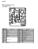
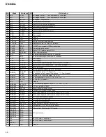
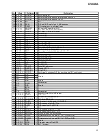
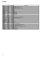
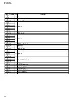
Pin Function
Pin
Input /
No.
Mnemonic
Output
Function
1–16
P0–P15
I
8-Bit or 16-Bit 4:2:2 Multiplexed YCrCb Pixel Port. The LSB of the input data is set up on
Pin P0.
17, 25, 29,
V
AA
P
Analog Power Supply (3.3 V to 5 V).
38, 43, 54,
63
18, 24, 26,
AGND
HSYNC
VSYNC
BLANK
G
Analog Ground.
33, 39, 42,
55, 64
19
I/O
(Modes 1, 2, and 3) Control Signal. This pin may be configured to be an output
(Master Mode) or an input (Slave Mode) and accept Sync Signals.
20
I/O
Control Signal. This pin may be configured as an output (Master Mode) or as an
input ( Slave Mode) and accept
as a Control Signal.
21
I/O
Video Blanking Control Signal. This signal is optional. For further information see Vertical
Blanking Data Insertion and
Input section.
22
ALSB
I
TTL Address Input. This signal sets up the LSB of the MPU address.
23
TTXREQ
O
T eletext Data Request Output Signal, used to control teletext data transfer.
27
CLKIN
I
TTL Clock Input. Requires a stable 27 MHz reference clock for standard operation. Alterna-
tively, a 24.5454 MHz (NTSC) or 29.5 MHz (PAL) can be used for square pixel operation.
28
CLKOUT
O
Clock Output Pin.
30
SCL
I
MPU Port Serial Interface Clock Input.
31
SDA
I/O
MPU Port Serial Data Input/Output.
32
SCRESET/
I
Multifunctional Input: Real-Time Control (RTC) Input, Timing Reset Input, Subcarrier Reset
RTC/TR
Input.
34
R
SET2
I
A 1200
Ω
resistor connected from this pin to ground is used to control full-scale amplitudes
of the Video Signals from DACs D , E, and F.
35
COMP 2
O
Compensation Pin for DACs D, E, and F. Connect a 0.1
µ
F Capacitor from COMP2 to V
AA
.
36
DAC F
O
S-Video C/V/RED Analog Output. This DAC is capable of providing 4.33 mA output.
37
DAC E
O
S-Video Y/U/BLUE Analog Output. This D AC is capable of providing 4.33 mA output.
40
DAC D
O
Composite/Y/GREEN Analog Output. This DAC is capable of providing 4.33 mA output.
41
DAC C
O
S-Video C/V/RED Analog Output. This DAC is capable of providing 4.33 mA output.
44
DAC B
O
S-Video Y/U/BLUE Analog Output. This DAC is capable of providing 4.33 mA output.
45
DAC A
O
Composite/Y/GREEN Analog Output. This DAC is capable of providing 4.33 mA output.
46
COMP 1
O
Compensation Pin for DACs A, B, and C. Connect a 0.1
µ
F Capacitor from COMP1 to V
AA
.
47
V
REF
I/O
Voltage Reference Input for DACs or Voltage Reference Output (1.235 V). An external
V
REF
cannot be used in 4 oversampling mode.
48
R
SET1
I
A 1200
Ω
resistor connected from this pin to ground is used to control full-scale amplitudes
of the Video Signals from DACs A, B, and C.
49
I
T he input resets the on-chip timing generator and sets the ADV7190/ADV7191 into default
mode. See Appendix 8 for Default Register settings.
50
O
D ual function
or
Output Sync Signal at TTL Level.
51
VSO/CLAMP
CSO_HSO
RESET
I/O
M ultifunction Pin.
Output Sync Signal at TTL level. CLAMP TTL Output Signals
can be used to drive external circuitry to enable clamping of all Video Signals.
52
PAL_NTSC
I
Input signal to select PAL or NTSC mode of operation, pin set to Logic 1 selects PAL.
53, 57–62
NC
No Connect.
56
TTX
I
T eletext Data Input Pin.
HSYNC
VSYNC
VSYNC
BLANK
HSO
VSO
CSO
Summary of Contents for DV-646A
Page 9: ...DV 646A 9 ...
Page 15: ...DV 646A 15 ...
Page 38: ...DV 646A 38 ...
Page 46: ...A B C D 1 2 3 4 1 2 3 4 46 DV 646A D 4 4 SCRB ASSY CN702 C VNP1838 A SIDE A SCRB ASSY D ...
Page 65: ...65 DV 646A DVDM ASSY B SIDE B TE FE ...
Page 101: ...101 DV 646A 8 PANEL FACILITIES AND SPECIFICATIONS 8 1 PANEL FACILITIES 8 1 1 Front Panel ...
Page 102: ...102 DV 646A 8 1 2 Remote Control ...
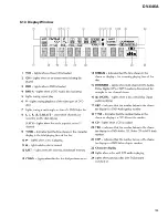
Page 103: ...103 DV 646A 8 1 3 Display Window ...

